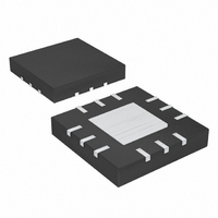
MAX8890ETCDDD+ Maxim Integrated Products, MAX8890ETCDDD+ Datasheet - Page 2

MAX8890ETCDDD+
Manufacturer Part Number
MAX8890ETCDDD+
Description
IC POWER MANAGE CELL 12-TQFN
Manufacturer
Maxim Integrated Products
Datasheet
1.MAX8890ETCAAAT.pdf
(12 pages)
Specifications of MAX8890ETCDDD+
Applications
Handheld/Mobile Devices
Current - Supply
180µA
Voltage - Supply
2.5 V ~ 5.5 V
Operating Temperature
-40°C ~ 85°C
Mounting Type
Surface Mount
Package / Case
12-TQFN Exposed Pad
Product
Charge Management
Battery Type
Li-Ion, Li-Polymer
Operating Supply Voltage
2.5 V to 5.5 V
Supply Current
180 uA
Maximum Operating Temperature
+ 85 C
Minimum Operating Temperature
- 40 C
Charge Safety Timers
No
Mounting Style
SMD/SMT
Temperature Monitoring
No
Uvlo Start Threshold
2.25 V
Uvlo Stop Threshold
2.25 V
Lead Free Status / RoHS Status
Lead free / RoHS Compliant
ABSOLUTE MAXIMUM RATINGS
IN_, EN_ to GND.......................................................-0.3V to +6V
OUT_, BP to GND ......................................-0.3V to (V
Output Short-Circuit Protection (Note A) .......................indefinite
Continuous Power Dissipation (T
Integrated Cellular RF-Section
Power-Management IC
Note A: As long as the maximum continuous power dissipation rating is not exceeded, the output can be shorted indefinitely.
Stresses beyond those listed under “Absolute Maximum Ratings” may cause permanent damage to the device. These are stress ratings only, and functional
operation of the device at these or any other conditions beyond those indicated in the operational sections of the specifications is not implied. Exposure to
absolute maximum rating conditions for extended periods may affect device reliability.
ELECTRICAL CHARACTERISTICS
(V
noted. Typical values are at T
2
12-Pin 4 x 4 QFN (derate 16.9mW/°C above +70°C) .......1349mW
GENERAL
Input Voltage
Input Undervoltage Lockout
Threshold
Input Undervoltage Hysteresis
SUPPLY CURRENT
Quiescent Supply Current
Shutdown Supply Current
LINEAR REGULATORS
Output Voltage Accuracy
Current Limit
Output Pulldown Resistance
Dropout Voltage (Note 1)
Line Regulation
Output Voltage Noise
Output Voltage PSRR
Channel-to-Channel Isolation
IN
_ = 3.6V, EN_ = IN_, C
_______________________________________________________________________________________
PARAMETER
IN
A
= 6.8µF, C
= +25°C.)
A
= +70°C)
SYMBOL
V
R
V
V
V
V
I
UVLO
OUT
OUT
OUT
IN
LIM
I
IN
Q
OUT
_ -
_
_
_
_
_ = 2.2µF, C
Rising and falling edge
I
EN_ = OUT_ = GND
V
highest of
(V
V
I
100mA
OUT_ = GND
EN_ = GND
I
I
I
V
2.4V, or V
2.4V, I
10Hz to 100kHz, C
V
100Hz, C
I
10kHz, C
I
OUT
OUT
OUT
OUT
OUT
OUT
OUT
IN
OUT3
IN
OUT
OUT1
IN
_ = 0.5V + the
_ = (V
_ = 0
_ = 1mA to
_ = 1mA
_ = 50mA
_ = 100mA
_ = 10mA
_ = 10mA
_ + 0.3V)
_ = 2.8V, I
),
OUT
, V
OUT
BP
OUT
OUT
OUT2
IN
= 1mA
_ = 2.5V to 5.5V for V
= 0.01µF, all ceramic capacitors T
_+ 0.1V) to 5.5V for V
_ = 2.2µF ceramic,
_ = 2.2µF ceramic,
, or
CONDITIONS
OUT
OUT
_ = 10mA
Operating Temperature Range ...........................-40°C to +85°C
Junction Temperature ......................................................+150°C
Storage Temperature Range .............................-65°C to +150°C
Lead Temperature (soldering, 10s) .................................+300°C
T
T
A
A
_ = 10µF ceramic,
= +85 C
= 0 C +85 C
OUT
OUT
_ <
_
A
-0.15
2.10
MIN
120
2.5
= 0°C to +85°C, unless otherwise
-1
-2
3
TYP
2.25
0.01
180
250
45
25
50
45
67
64
5
1
+0.15
MAX
2.45
330
500
100
5.5
10
+1
+2
8
UNITS
µV
%/V
mV
mA
mV
µA
µA
k
dB
dB
%
V
V
RMS


