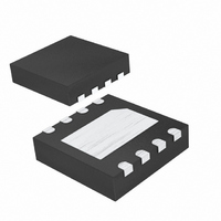
MAX1946ETA+T Maxim Integrated Products, MAX1946ETA+T Datasheet - Page 11

MAX1946ETA+T
Manufacturer Part Number
MAX1946ETA+T
Description
IC SW USB SNGL W/FB 8-TDFN
Manufacturer
Maxim Integrated Products
Datasheet
1.MAX1946ETAT.pdf
(13 pages)
Specifications of MAX1946ETA+T
Applications
USB, Peripherals
Current - Supply
40µA
Voltage - Supply
2.7 V ~ 5.5 V
Operating Temperature
-40°C ~ 85°C
Mounting Type
Surface Mount
Package / Case
8-TDFN Exposed Pad
Lead Free Status / RoHS Status
Lead free / RoHS Compliant
Figure 2. Typical Application Circuit
Bypass OUT to GND with a 1µF ceramic capacitor for
local decoupling. Additional bulk capacitance (up to
470µF) reduces output-voltage transients under dynamic
load conditions. Using output capacitors greater than
470µF can assert FAULT if the current limit cannot
charge the output capacitor within the 20ms fault-
blanking period. In addition to bulk capacitance, small-
value (0.1µF or greater) ceramic capacitors improve
the output’s resilience to electrostatic discharge (ESD).
A wide variety of devices (mice, keyboards, cameras, and
printers) typically connect to the USB port with cables,
which can add an inductive component to the load. This
inductance causes the output voltage at the USB port to
oscillate during a load step. The MAX1946 drives induc-
tive loads, but avoid exceeding the device’s absolute
maximum ratings. The load inductance is usually relatively
small, and the MAX1946 input typically includes substan-
tial bulk capacitance from an upstream regulator as well
as local bypass capacitors, limiting overshoot. If severe
ringing occurs due to large load inductance, clamp the
MAX1946 output below +6V and above -0.3V.
When turned on, the MAX1946 output ramps up over
1.2ms to eliminate load transients on the upstream
power source. When turned off, the output ramps down
for 3ms. Under fault conditions, the output of the
MAX1946 turns off rapidly to provide maximum safety
for the upstream power source and downstream
devices. Internal blocks shut down to minimize supply
current when the switch is off.
2.7V TO 5.5V
INPUT
*USB APPLICATIONS MAY REQUIRE
ADDITIONAL BULK CAPACITANCE
0.1µF
ON
OFF
______________________________________________________________________________________
Turn-On and Turn-Off Behavior
Single USB Switch with Autoreset and
ON
SEL
IN
IN
MAX1946
Driving Inductive Loads
GND
FAULT
Output Capacitor
OUT
OUT
100kΩ
Fault Blanking in Tiny TDFN
1µF
Keep all traces as short as possible to reduce the effect
of undesirable parasitic inductance, and to optimize the
switch response time to output short-circuit conditions.
Place input and output capacitors no more than 5mm
from device leads. Connect IN and OUT to the power
bus with short traces. The exposed pad on the TDFN
package underside must be soldered to the PC board in
order to realize the rated package dissipation.
An active switch dissipates little power with minimal
change in package temperature. Calculate the power
dissipation for this condition as follows:
At the normal operating current (I
maximum on-resistance of the switch (90mΩ), the
power dissipation is:
The worst-case power dissipation occurs when the out-
put current is just below the current-limit threshold
(1.2A max) with an output voltage just greater than 1V.
In this case, the power dissipated is the voltage drop
across the switch multiplied by the current limit:
For a 5V input and 1V output, the maximum power dis-
sipation per switch is:
Since the package power dissipation is 1951mW for the
8-pin TDFN, the MAX1946 die temperature exceeds the
+160°C thermal-shutdown threshold. The switch output
shuts down until the junction temperature cools by
15°C. The duty cycle and period are strong functions of
the ambient temperature and the PC board layout (see
the Thermal Shutdown section).
If the output current exceeds the current-limit threshold,
or the output voltage is pulled below the short-circuit
detect threshold, the MAX1946 enters a fault state after
20ms, at which point autoreset mode is enabled and
25mA is sourced by the output. For a 5V input, OUT
short-circuited to GND, and autoreset mode active, the
power dissipation is as follows:
P = (0.5A)
P = 1.2A
P = 0.025A
P = I
P = (I
LIM
Layout and Thermal Dissipation
2
OUT
(5V - 1V) = 4.8W
0.09Ω = 22.5mW
(V
5V = 0.125W
)
2
IN
- V
R
ON
OUT
OUT
)
= 0.5A) and the
11


