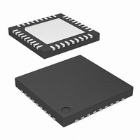
ISL97651ARTZ-TK Intersil, ISL97651ARTZ-TK Datasheet - Page 18

ISL97651ARTZ-TK
Manufacturer Part Number
ISL97651ARTZ-TK
Description
IC LCD SUPPLY HP 4CHN 36-TQFN
Manufacturer
Intersil
Datasheet
1.ISL97651ARTZ-TK.pdf
(19 pages)
Specifications of ISL97651ARTZ-TK
Applications
LCD TV/Monitor
Current - Supply
400µA
Voltage - Supply
4 V ~ 5.5 V
Operating Temperature
-40°C ~ 105°C
Mounting Type
Surface Mount
Package / Case
36-TQFN
Lead Free Status / RoHS Status
Lead free / RoHS Compliant
After C
turned-on and produces an initial current output of
IDELB_ON1 (~50µA). This current allows the user to control
the turn-on inrush current into the A
capacitors by a suitable choice of C4. This capacitor can
provide extra delay and also filter out any noise coupled into
the gate of M0, avoiding spurious turn-on, however, C4 must
not be so large that it prevents DELB reaching 0.6V by the
end of the start-up sequence on C
ramp on C
for C4. The 0.6V threshold is used by the chip's fault
detection system and if V(DELB) is still above 0.6V at the
end of the power sequencing then a fault time-out ramp will
be initiated on C
When the voltage at DELB falls below ~0.6V it's current is
increased to IDELB_ON2 (~1.4mA) to firmly pull the DELB
voltage to ground.
If the maximum V
voltage being used, then a resistor may be inserted between
the DELB pin and the gate of M0 such that it's potential
divider action with R4 ensures the gate/source stays below
VGS(M0)max. This additional resistor allows much larger
values of C4 to be used, and hence longer A
without affecting the fault protection on DELB.
Component Selection for Start-up Sequencing and
Fault Protection
The C
to stabilize the V
22nF to 1µF and should not be more than five times the
capacitor on C
The C
range from 47nF minimum to several microfarads – only
limited by the leakage in the capacitor reaching µA levels.
C
above). Note with 220nF on C
typically 50ms and the use of a larger/smaller value will vary
this time proportionally (e.g., 1µF will give a fault time-out
period of typically 230ms).
Intersil products are sold by description only. Intersil Corporation reserves the right to make changes in circuit design, software and/or specifications at any time without
notice. Accordingly, the reader is cautioned to verify that data sheets are current before placing orders. Information furnished by Intersil is believed to be accurate and
reliable. However, no responsibility is assumed by Intersil or its subsidiaries for its use; nor for any infringements of patents or other rights of third parties which may result
from its use. No license is granted by implication or otherwise under any patent or patent rights of Intersil or its subsidiaries.
DEL
REF
DEL
should be at least 1/5 of the value of C
DLY
DLY
capacitor is typically 220nF and has a usable
capacitor is typically set at 220nF and is required
reaches the 4th peak, the internal N-FET is
DEL
All Intersil U.S. products are manufactured, assembled and tested utilizing ISO9000 quality systems.
will start. A value of 22nF is typically required
DLY
REF
GS
to ensure correct start-up operation.
Intersil Corporation’s quality certifications can be viewed at www.intersil.com/design/quality
.
voltage of M0 is less than the A
output. The range of C
For information regarding Intersil Corporation and its products, see www.intersil.com
18
DEL
DLY
the fault time-out will be
VDD_delay
, else a fault time-out
REF
VDD
REF
supply
is from
delay,
(see
VDD
ISL97651
Over-Temperature Protection
An internal temperature sensor continuously monitors the
die temperature. In the event that the die temperature
exceeds the thermal trip point of +150°C, the device will shut
down. Operation with die temperatures between +125°C and
+150°C can be tolerated for short periods of time, however,
in order to maximize the operating life of the IC, it is
recommended that the effective continuous operating
junction temperature of the die should not exceed +125°C.
Layout Recommendation
The device’s performance including efficiency, output noise,
transient response and control loop stability is dramatically
affected by the PCB layout. PCB layout is critical, especially
at high switching frequency.
There are some general guidelines for layout:
A demo board is available to illustrate the proper layout
implementation.
1. Place the external power components (the input
2. Place V
3. Reduce the loop with large AC amplitudes and fast slew
4. The feedback network should sense the output voltage
5. The power ground (PGND) and signal ground (SGND)
6. The exposed die plate, on the underneath of the
7. To minimize the thermal resistance of the package when
8. Minimize feedback input track lengths to avoid switching
capacitors, output capacitors, boost inductor and output
diodes, etc.) in close proximity to the device. Traces to
these components should be kept as short and wide as
possible to minimize parasitic inductance and resistance.
rate.
directly from the point of load, and be as far away from LX
node as possible.
pins should be connected at only one point.
package, should be soldered to an equivalent area of
metal on the PCB. This contact area should have multiple
via connections to the back of the PCB as well as
connections to intermediate PCB layers, if available, to
maximize thermal dissipation away from the IC.”
soldered to a multi-layer PCB, the amount of copper track
and ground plane area connected to the exposed die
plate should be maximized and spread out as far as
possible from the IC. The bottom and top PCB areas
especially should be maximized to allow thermal
dissipation to the surrounding air.
noise pick-up.
REF
and V
DC
bypass capacitors close to the pins.
April 24, 2009
FN7493.3


