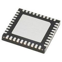
IR3523MTRPBF International Rectifier, IR3523MTRPBF Datasheet - Page 15

IR3523MTRPBF
Manufacturer Part Number
IR3523MTRPBF
Description
IC XPHASE3 CTLR VR11.1 40-MLPQ
Manufacturer
International Rectifier
Series
XPhase3™r
Datasheet
1.IR3523MTRPBF.pdf
(37 pages)
Specifications of IR3523MTRPBF
Applications
Processor
Current - Supply
10mA
Voltage - Supply
4.75 V ~ 7.5 V
Operating Temperature
0°C ~ 100°C
Mounting Type
Surface Mount
Package / Case
40-MLPQ
Ic Function
Dual Output Control IC
Supply Voltage Range
4.75V To 7.5V
Operating Temperature Range
0°C To +150°C
Digital Ic Case Style
MLPQ
No. Of Pins
40
Controller Type
XPhase
Rohs Compliant
Yes
Package
40-Lead MLPQ
Circuit
X-Phase Control IC
Switch Freq (khz)
250kHz to 1.5MHz
Pbf
PbF Option Available
Lead Free Status / RoHS Status
Lead free / RoHS Compliant
IR3523 THEORY OF OPERATION
Block Diagram
The Block diagram of the IR3523 is shown in Figure 3, and specific features are discussed in the following sections.
All the features are described using one output but suitable for both unless otherwise specified.
VIDx Control
The IR3523 converter outputs are independently controlled by two three-bit input interfaces (see Table 1-2): VDAC1
(VOUT1) and VDAC2 (VOUT2). The VID codes are stored and then inputted to the Digital-to-Analog Converter
(DAC) whose output is sent to the VDAC buffer amplifier. The output of the buffer amplifier is the VDAC pin.
VDAC1 will initially boot to 1.1V when Vout1 is enabled then will transition to the stored VID1 value once SS/DEL1
reached 3.0 V. The VDAC voltage, input offsets of error amplifier and remote sense differential amplifier, are post-
package trimmed to provide 0.5% system set-point accuracy. The actual VDAC voltage does not determine the
system accuracy, which has a wider tolerance. The VID pins, VID2_x and VID1_x, require an external bias voltage
and should not be floated.
The IR3523 can accept changes in the VID code while operating and vary DAC voltage accordingly. The
sink/source capability of the VDAC buffer amplifier is programmed by the same external resistor that sets the
oscillator frequency. The slew rate of the voltage at the VDAC pins can be adjusted by the external capacitors
between VDAC pins and LGND pin. A resistor connected in series with this capacitor is required to compensate the
VDAC buffer amplifiers. The stepped VID transition results in a smooth analog transition of the VDAC voltage and
converter output voltage. This analog transition minimizes inrush currents in the input (and output) capacitors and
reduces overshoot of the output voltage.
Page 15 of 37
VID1_4
VID2_2
Table 2: Output (2) 3-bit VID table
Table 1: Output (1) 3-bit VID table
0
0
0
0
1
1
1
1
0
0
0
0
1
1
1
1
VID1_3
VID2_1
0
0
1
1
0
0
1
1
0
0
1
1
0
0
1
1
VID1_2
VID2_0
0
1
0
1
0
1
0
1
0
1
0
1
0
1
0
1
VDAC1
VDAC2
1.200
1.175
1.150
1.125
1.100
1.075
1.050
1.025
1.350
1.400
1.450
1.500
1.550
1.600
1.650
1.800
June 20, 2008
IR3523


