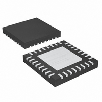
MAX1517ETJ+ Maxim Integrated Products, MAX1517ETJ+ Datasheet - Page 22

MAX1517ETJ+
Manufacturer Part Number
MAX1517ETJ+
Description
IC DC/DC CONV TFT-LCD 32-TQFN
Manufacturer
Maxim Integrated Products
Datasheet
1.MAX1517ETJ.pdf
(26 pages)
Specifications of MAX1517ETJ+
Applications
LCD Display, Automotive
Voltage - Supply
2.6 V ~ 5.5 V
Operating Temperature
-40°C ~ 85°C
Mounting Type
Surface Mount
Package / Case
32-TQFN Exposed Pad
Lead Free Status / RoHS Status
Lead free / RoHS Compliant
Current - Supply
-
Lead Free Status / Rohs Status
Lead free / RoHS Compliant
TFT-LCD DC-DC Converters with
Operational Amplifiers
Figure 9. Positive Charge-Pump Output Voltage vs. V
Adjust the gate-off linear-regulator REG N output volt-
age by connecting a resistive voltage-divider from
V
(Figure 1). Select R8 in the range of 20kΩ to 50kΩ.
Calculate R7 with the following equation:
where V
only source up to 50µA; using a resistor less than 20kΩ
for R8 results in higher bias current than REF can supply.
The pass transistor must meet specifications for current
gain (h
voltage and power dissipation. The transistor’s current
gain limits the guaranteed maximum output current to:
where I
rent, V
age drop, and R
between the transistor’s base and emitter. Furthermore,
the transistor’s current gain increases the linear regula-
tor’s DC loop gain (see the Stability Requirements sec-
tion), so excessive gain destabilizes the output.
22
GOFF
______________________________________________________________________________________
BE
FE
DRV
to REF with the center tap connected to FBN
FBN
), input capacitance, collector-emitter saturation
I
is the transistor’s base-to-emitter forward volt-
LOAD MAX
is the minimum guaranteed base-drive cur-
= 250mV, V
60
50
40
30
20
10
0
2
(
V
2-STAGE CHARGE PUMP
D
R
BE
= 0.3V TO 1V
7
OUTPUT VOLTAGE vs. V
4
)
=
POSITIVE CHARGE-PUMP
is the pullup resistor connected
=
R
8
REF
I
DRV
×
6
V
V
V
3-STAGE CHARGE PUMP
FBN
Pass-Transistor Selection
1-STAGE CHARGE PUMP
= 1.25V. Note that REF can
MAIN
REF
−
8
R
V
(V)
−
BE
BE
−
V
V
10
GOFF
×
FBN
MAIN
h
FE MIN
12
(
14
)
MAIN
Therefore, transistors with current gain over 100 at the
maximum output current can be difficult to stabilize and
are not recommended unless the high gain is needed to
meet the load-current requirements.
The transistor’s saturation voltage at the maximum out-
put current determines the minimum input-to-output
voltage differential that the linear regulator can support.
Also, the package’s power dissipation limits the usable
maximum input-to-output voltage differential. The maxi-
mum power-dissipation capability of the transistor’s
package and mounting must exceed the actual power
dissipated in the device. The power dissipated equals
the maximum load current (I
by the maximum input-to-output voltage differential:
where V
linear regulator, and V
the linear regulator.
The MAX1516/MAX1517/MAX1518 linear-regulator con-
trollers use an internal transconductance amplifier to
drive an external pass transistor. The transconductance
amplifier, the pass transistor, the base-emitter resistor,
and the output capacitor determine the loop stability.
The following applies to both linear-regulator controllers
in the MAX1516/MAX1517/MAX1518.
Figure 10. Negative Charge-Pump Output Voltage vs. V
P I
=
IN(MAX)_LR
LOAD MAX LR
-10
-15
-20
-25
-30
-35
-40
-45
-0
-5
(
2
CHARGE PUMP
V
D
CHARGE PUMP
= 0.3V TO 1V
is the maximum input voltage of the
OUTPUT VOLTAGE vs. V
)_
2-STAGE
NEGATIVE CHARGE-PUMP
4
OUT
3-STAGE
×
6
(
V
_
V
IN MAX LR
LR
MAIN
LOAD(MAX)_LR
(
8
Stability Requirements
is the output voltage of
(V)
)_
10
1-STAGE
CHARGE PUMP
MAIN
−
12
V
OUT LR
) multiplied
14
_
MAIN
)


