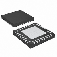
MAX1517ETJ+ Maxim Integrated Products, MAX1517ETJ+ Datasheet - Page 20

MAX1517ETJ+
Manufacturer Part Number
MAX1517ETJ+
Description
IC DC/DC CONV TFT-LCD 32-TQFN
Manufacturer
Maxim Integrated Products
Datasheet
1.MAX1517ETJ.pdf
(26 pages)
Specifications of MAX1517ETJ+
Applications
LCD Display, Automotive
Voltage - Supply
2.6 V ~ 5.5 V
Operating Temperature
-40°C ~ 85°C
Mounting Type
Surface Mount
Package / Case
32-TQFN Exposed Pad
Lead Free Status / RoHS Status
Lead free / RoHS Compliant
Current - Supply
-
Lead Free Status / Rohs Status
Lead free / RoHS Compliant
TFT-LCD DC-DC Converters with
Operational Amplifiers
The total output voltage ripple has two components: the
capacitive ripple caused by the charging and discharg-
ing of the output capacitance, and the ohmic ripple due
to the capacitor’s equivalent series resistance (ESR).
where I
Inductor Selection section). For ceramic capacitors, the
output voltage ripple is typically dominated by
V
teristics of the output capacitor must also be considered.
The input capacitor (C
drawn from the input supply and reduces noise injec-
tion into the IC. A 22µF ceramic capacitor is used in the
Typical Applications Circuit (Figure 1) because of the
high source impedance seen in typical lab setups.
Actual applications usually have much lower source
impedance since the step-up regulator often runs
directly from the output of another regulated supply.
Typically, C
the Typical Applications Circuit. Ensure a low-noise
supply at IN by using adequate C
greater voltage variation can be tolerated on C
decoupled from C
R10 and C18 in Figure 1).
The MAX1516/MAX1517/MAX1518s’ high switching fre-
quency demands a high-speed rectifier. Schottky
diodes are recommended for most applications
because of their fast recovery time and low forward
voltage. In general, a 2A Schottky diode complements
the internal MOSFET well.
The output voltage of the main step-up regulator can be
adjusted by connecting a resistive voltage-divider from
the output (V
ed to FB (see Figure 1). Select R2 in the 10kΩ to 50kΩ
range. Calculate R1 with the following equation:
20
RIPPLE(C)
______________________________________________________________________________________
PEAK
V
V
V
RIPPLE
RIPPLE C
RIPPLE ESR
. The voltage rating and temperature charac-
IN
MAIN
can be reduced below the values used in
is the peak inductor current (see the
( )
(
=
) to AGND with the center tap connect-
R
V
1
IN
≈
RIPPLE C
)
=
C
I
≈
MAIN
R
using an RC lowpass filter (see
OUT
I
2
PEAK ESR COUT
IN
×
) reduces the current peaks
( )
Output-Capacitor Selection
V
Input-Capacitor Selection
R
Output-Voltage Selection
V
MAIN
V
+
V
MAIN
FB
MAIN OSC
V
RIPPLE ESR
(
−
f
−
1
V
IN
(
IN
)
Rectifier Diode
. Alternately,
,
)
and
IN
if IN is
where V
is 1.236V. Place R1 and R2 close to the IC.
The maximum output voltage of the step-up regulator is
13V, which is limited by the absolute maximum rating of
the internal power MOSFET. To achieve higher output
voltages, an external n-channel MOSFET can be cascod-
ed with the internal FET (Figure 8). Since the gate of the
external FET is biased from the input supply, use a logic-
level FET to ensure that the FET is fully enhanced at the
minimum input voltage. The current rating of the FET
needs to be higher than the IC’s internal current limit.
Choose R
gain for fast transient response. Choose C
the integrator zero to maintain loop stability.
For low-ESR output capacitors, use the following equa-
tions to obtain stable performance and good transient
response:
To further optimize transient response, vary R
20% steps and C
transient-response waveforms.
For highest efficiency, always choose the lowest num-
ber of charge-pump stages that meet the output
requirement. Figures 9 and 10 show the positive and
negative charge-pump output voltages for a given
V
The number of positive charge-pump stages is given by:
where n
stages, V
put, V
the forward-voltage drop of the charge-pump diode,
and V
ulator. Use V
MAIN
DROPOUT
MAIN
Selecting the Number of Charge-Pump Stages
for one-, two-, and three-stage charge pumps.
FB
POS
GON
n
COMP
R
C
, the step-up regulator’s feedback set point,
POS
is the main step-up regulator output, V
COMP
COMP
DROPOUT
is the number of positive charge-pump
is the gate-on linear-regulator REG P out-
=
is the dropout margin for the linear reg-
to set the high-frequency integrator
V
COMP
≈
≈
GON
Generating Output Voltages >13V
315
10
= 0.3V.
×
+
V
×
I
MAIN MAX
in 50% steps while observing
MAIN
L I
V
V
V
DROPOUT
IN
×
OUT
MAIN MAX
×
(
− ×
V
×
2
OUT
C
(
Loop Compensation
)
OUT
V
×
D
−
×
Charge Pumps
R
V
C
)
COMP
MAIN
OUT
COMP
COMP
to set
D
in
is


