LP3906SQ-PPXP/NOPB National Semiconductor, LP3906SQ-PPXP/NOPB Datasheet - Page 8
LP3906SQ-PPXP/NOPB
Manufacturer Part Number
LP3906SQ-PPXP/NOPB
Description
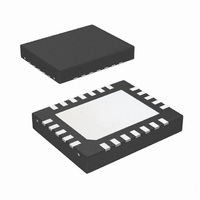
IC REG DC-DC/LINEAR DUAL 24-LLP
Manufacturer
National Semiconductor
Series
PowerWise®r
Datasheet
1.LP3906SQ-DJXINOPB.pdf
(40 pages)
Specifications of LP3906SQ-PPXP/NOPB
Applications
Digital Cores
Current - Supply
60µA
Voltage - Supply
2.7 V ~ 5.5 V
Operating Temperature
-40°C ~ 85°C
Mounting Type
Surface Mount
Package / Case
24-LLP
For Use With
LP3906SQ-JXXIEV - BOARD EVALUATION LP3906SQ-JXXI
Lead Free Status / RoHS Status
Lead free / RoHS Compliant
Other names
LP3906SQ-PPXPTR
Available stocks
Company
Part Number
Manufacturer
Quantity
Price

Part Number:
LP3906SQ-PPXP/NOPB
Manufacturer:
NS/国半
Quantity:
20 000


www.national.com
V
V
IL
IH
IO Electrical Characteristics
Unless otherwise noted: Typical values and limits appearing in normal type apply for T
type apply over the entire junction temperature range for operation, T
Note 1: Absolute Maximum Ratings indicate limits beyond which damage to the component may occur. Operating Ratings are conditions under which operation
of the device is guaranteed. Operating Ratings do not imply guaranteed performance limits. For guaranteed performance limits and associated test conditions,
see the Electrical Characteristics.
Note 2: All voltages are with respect to the potential at the GND pin.
Note 3: Internal thermal shutdown circuitry protects the device from permanent damage. Thermal shutdown engages at T
= 140°C (typ.)
Note 4: The Human body model is a 100 pF capacitor discharged through a 1.5 kΩ resistor into each pin. (MILSTD - 883 3015.7)
Note 5: In applications where high power dissipation and/or poor package thermal resistance is present, the maximum ambient temperature may have to be
derated. Maximum ambient temperature (T
dissipation of the device in the application (P
following equation: T
Note 6: Junction-to-ambient thermal resistance is highly application and board-layout dependent. In applications where high maximum power dissipation exists,
special care must be paid to thermal dissipation issues in board design.
Note 7: Min and Max limits are guaranteed by design, test, or statistical analysis. Typical numbers are not guaranteed, but do represent the most likely norm.
Note 8: C
Note 9: The device maintains a stable, regulated output voltage without a load.
Note 10: Dropout voltage is the voltage difference between the input and the output at which the output voltage drops to 100 mV below its nominal value.
Note 11: Quiescent current is defined here as the difference in current between the input voltage source and the load at V
Note 12: V
Note 13: This specification is guaranteed by design.
Note 14: The Iq can be defined as the standing current of the LP3906 when the I2C bus is active and all other power blocks have been disabled via the I2C bus,
or it can be defined as the I2C bus active, and the other power blocks are active under no load condition. These two values can be used by the system designer
when the LP3906 is powered using a battery. If the user plans to use the HW enable pins to disable each block of the IC please contact the factory applications
for IQ details.
Note 15: Pins 13, 19 can operate from Vin min of 1.74 to a Vin max of 5.5V this rating is only for the series pass pmos power fet. It allows the system design to
use a lower voltage rating if the input voltage comes from a buck output.
Note 16: The Iq exhibits a higher current draw when the EN pin is de-asserted because the I2C buffer pins draw an additional 2µA
Symbol
IN
IN
, C
minimum for line regulation values is 1.8V.
OUT
Input Low Level
Input High Level
: Low-ESR Surface-Mount Ceramic Capacitors (MLCCs) used in setting electrical characteristics.
A-MAX
= T
J-MAX-OP
Parameter
− (θ
JA
A-MAX
D-MAX
× P
) is dependent on the maximum operating junction temperature (T
D-MAX
), and the junction-to-ambient thermal resistance of the part/package in the application (θ
). See applications section.
8
J
= 0°C to +125°C.
Conditions
J
= 25°C. Limits appearing in boldface
(Note
J-MAX-OP
13)
J
OUT
= 125°C), the maximum power
= 160°C (typ.) and disengages at T
.
Min
1.2
Limit
JA
Max
), as given by the
0.4
Units
V
V
J
Related parts for LP3906SQ-PPXP/NOPB
Image
Part Number
Description
Manufacturer
Datasheet
Request
R

Part Number:
Description:
IC REG DC-DC/LINEAR DUAL 24-LLP
Manufacturer:
National Semiconductor
Datasheet:
Part Number:
Description:
IC REG DC-DC/LINEAR DUAL 24-LLP
Manufacturer:
National Semiconductor
Datasheet:
Part Number:
Description:
IC REG DC-DC/LINEAR DUAL 24-LLP
Manufacturer:
National Semiconductor
Datasheet:

Part Number:
Description:
BOARD EVALUATION LP3906SQ-JXXI
Manufacturer:
National Semiconductor
Datasheet:
Part Number:
Description:
EVAL BOARD FOR LP3906SQ-JXXI
Manufacturer:
National Semiconductor
Datasheet:
Part Number:
Description:
IC REG DC-DC/LINEAR DUAL 24-LLP
Manufacturer:
National Semiconductor
Datasheet:
Part Number:
Description:
IC REG BUCK/LDO DUAL 1.5A 300MA
Manufacturer:
National Semiconductor
Datasheet:
Part Number:
Description:
National Semiconductor [8-Bit D/A Converter]
Manufacturer:
National Semiconductor
Datasheet:
Part Number:
Description:
National Semiconductor [Media Coprocessor]
Manufacturer:
National Semiconductor
Datasheet:
Part Number:
Description:
Digitally Controlled Tone and Volume Circuit with Stereo Audio Power Amplifier, Microphone Preamp Stage and National 3D Sound
Manufacturer:
National Semiconductor
Datasheet:
Part Number:
Description:
Digitally Controlled Tone and Volume Circuit with Stereo Audio Power Amplifier, Microphone Preamp Stage and National 3D Sound
Manufacturer:
National Semiconductor
Datasheet:
Part Number:
Description:
AC97 Rev 2 Codec with Sample Rate Conversion and National 3D Sound
Manufacturer:
National Semiconductor
Part Number:
Description:
Manufacturer:
National Semiconductor
Datasheet:
Part Number:
Description:
Manufacturer:
National Semiconductor
Datasheet: