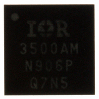
IR3500AMTRPBF International Rectifier, IR3500AMTRPBF Datasheet - Page 10

IR3500AMTRPBF
Manufacturer Part Number
IR3500AMTRPBF
Description
IC CTRL XPHASE3 VR11.0 32-MLPQ
Manufacturer
International Rectifier
Series
XPhase3™r
Datasheet
1.IR3500AMTRPBF.pdf
(48 pages)
Specifications of IR3500AMTRPBF
Applications
Processor
Current - Supply
6.5mA
Voltage - Supply
4.75 V ~ 7.5 V
Operating Temperature
0°C ~ 100°C
Mounting Type
Surface Mount
Package / Case
32-MLPQ
Package
32-Lead MLPQ
Circuit
X-Phase Control IC
Switch Freq (khz)
250kHz to 1.5MHz
Pbf
PbF Option Available
Lead Free Status / RoHS Status
Lead free / RoHS Compliant
Other names
IR3500AMTRPBFTR
second phase IC, etc. and PHSOUT of the last phase IC is connected back to PHSIN of the control IC. During
power up, the control IC sends out clock signals from both CLKOUT and PHSOUT pins and detects the feedback at
PHSIN pin to determine the phase number and monitor any fault in the daisy chain loop. Figure 5 shows the phase
timing for a four phase converter. The switching frequency is set by the resistor ROSC as shown in Figure 23. The
clock frequency equals the number of phase times the switching frequency.
PWM Operation
The PWM comparator is located in the phase IC. Upon receiving the falling edge of a clock pulse, the PWM latch is
set; the PWM ramp voltage begins to increase; the low side driver is turned off, and the high side driver is then
turned on after the non-overlap time. When the PWM ramp voltage exceeds the error amplifier’s output voltage the
PWM latch is reset. This turns off the high side driver, then turns on the low side driver after the non-overlap time,
and activates the ramp discharge clamp. The ramp discharge clamp quickly discharges the PWM ramp capacitor to
the output voltage of the share adjust amplifier in the phase IC until the next clock pulse.
The PWM latch is reset dominant allowing all phases to go to zero duty cycle within a few tens of nanoseconds in
response to a load step decrease. Phases can overlap and go up to 100% duty cycle in response to a load step
increase with turn-on gated by the clock pulses. An error amplifier output voltage greater than the common mode
input range of the PWM comparator results in 100% duty cycle regardless of the voltage of the PWM ramp. This
arrangement guarantees the error amplifier is always in control and can demand 0 to 100% duty cycle as required.
It also favors response to a load step decrease which is appropriate given the low output to input voltage ratio of
most systems. The inductor current will increase much more rapidly than decrease in response to load transients.
An additional advantage of the architecture is that differences in ground or input voltage at the phases have no
effect on operation since the PWM ramps are referenced to VDAC. Figure 6 depicts PWM operating waveforms
under various conditions
Control IC CLKOUT
(Phase IC CLKIN)
Control IC PHSOUT
(Phase IC1 PHSIN)
Phase IC1
PWM Latch SET
Phase IC 1 PHSOUT
(Phase IC2 PHSIN)
Phase IC 2 PHSOUT
(Phase IC3 PHSIN)
Phase IC 3 PHSOUT
(Phase IC4 PHSIN)
Phase IC4 PHSOUT
(Control IC PHSIN)
Page 10 of 48
Figure 5 - Four Phase Oscillator Waveforms
July 28, 2009
IR3500A


