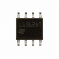
L6562ATDTR STMicroelectronics, L6562ATDTR Datasheet - Page 7

L6562ATDTR
Manufacturer Part Number
L6562ATDTR
Description
IC PFC CTRLR TRANSITION 8SOIC
Manufacturer
STMicroelectronics
Specifications of L6562ATDTR
Mode
Discontinuous (Transition)
Frequency - Switching
1MHz
Current - Startup
30µA
Voltage - Supply
10.5 V ~ 22.5 V
Operating Temperature
-25°C ~ 125°C
Mounting Type
Surface Mount
Package / Case
8-SOIC (3.9mm Width)
Output Voltage
10.3 V
Output Current
0.8 A
Input Voltage
10.5 V to 22.5 V
Operating Temperature Range
- 40 C to + 150 C
Mounting Style
SMD/SMT
For Use With
497-9018 - DIMMABLE 80W OFFLINE LED DRIVER
Lead Free Status / RoHS Status
Lead free / RoHS Compliant
Other names
497-8928-2
Available stocks
Company
Part Number
Manufacturer
Quantity
Price
Part Number:
L6562ATDTR
Manufacturer:
ST
Quantity:
20 000
Electrical characteristics
Table 5.
1. All the parameters are in tracking
2. The multiplier output is given by:
3. Parameters guaranteed by design, functionality tested in production.
7/25
Output overvoltage
Current sense comparator
Zero current detector
Starter
Gate driver
Symbol
Vcs
V
I
V
I
V
V
t
V
td
ZCDsnk
ZCDsrc
I
I
START
I
Oclamp
I
V
Hys
t
V
ZCDb
snkpk
V
srcpk
ZCDH
ZCDA
OVP
I
ZCDL
ZCDT
LEB
(H-L)
CS
OH
t
CS
OL
t
offset
r
f
Hysteresis
Dynamic OVP triggering
current
Static OVP threshold
Input bias current
Leading edge blanking
Delay to output
Current sense clamp
Current sense offset
Upper clamp voltage
Lower clamp voltage
Arming voltage
(positive-going edge)
Triggering voltage
(negative-going edge)
Input bias current
Source current capability
Sink current capability
Start timer period
Output low voltage
Output high voltage
Peak source current
Peak sink current
Voltage fall time
Voltage rise time
Output clamp voltage
UVLO saturation
Electrical characteristics (continued)
Parameter
V
cs
=
K
(3)
(1)
V
V
V
V
I
I
(3)
(3)
V
I
I
I
Vcc = 0 to V
ZCD
ZCD
sink
source
source
CS
COMP
MULT
MULT
ZCD
⋅
V
MULT
= 100 mA
= 0
= 2.5 mA
= - 2.5 mA
= 1 to 4.5 V
= 5 mA
= 5 mA; Vcc = 20 V
= 0
= 2.5 V
= Upper clamp, Vmult = 1.5 V
⋅
(
V
Test condition
CCon
COMP
, I
sink
−
2
5 .
= 2 mA
)
19.5
Min
100
-0.5
-1.5
-0.6
2.1
1.0
5.0
1.5
9.5
0.8
75
10
2.25
1.08
10.3
Typ
200
175
190
5.7
1.4
0.7
0.6
27
20
25
30
60
12
5
0
2
Max
30.5
1.16
300
300
130
2.4
6.5
0.5
1.2
1.1
70
15
-1
L6562AT
Unit
mV
mA
mA
µA
µA
µA
µA
ns
ns
ns
ns
µs
V
V
V
V
V
V
V
V
A
A
V
V


