PIP401,118 NXP Semiconductors, PIP401,118 Datasheet - Page 2
PIP401,118
Manufacturer Part Number
PIP401,118
Description
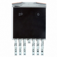
IC OR-ING INTEL SW D2PAK
Manufacturer
NXP Semiconductors
Datasheet
1.PIP401118.pdf
(16 pages)
Specifications of PIP401,118
Applications
CompactPCI™ High Reliability Power Supply Networks
Number Of Outputs
1
Internal Switch(s)
Yes
Delay Time - On
7µs
Delay Time - Off
200ns
Voltage - Supply
6.3 V ~ 20 V
Current - Supply
3mA
Operating Temperature
-40°C ~ 150°C
Mounting Type
Surface Mount
Package / Case
D²Pak, TO-263 (6 leads + tab)
Lead Free Status / RoHS Status
Lead free / RoHS Compliant
Fet Type
-
Other names
568-2326-2
934057294118
PIP401 /T3
934057294118
PIP401 /T3


Philips Semiconductors
5. Block diagram
6. Pinning information
Table 2:
7. Functional description
9397 750 10578
Product data
Symbol Pin
TFL
V
GND
VO
VRS
VI
CC
1
2
3
4, mb
5
6, 7
Pinning
I/O
O
-
-
O
I
I
Figure 1
functional blocks:
Figure 2
connected to VI. The output (VO) is connected to the system bus. An auxiliary supply
biases V
Description
overtemperature flag
positive supply voltage
ground
output
remote sense
input
•
•
•
•
Fig 1. Block diagram.
High-speed comparator with remote sense input
Power switch driver stage
Series power switch with very low on-state resistance
Overtemperature detection circuit with open collector output.
CC
shows the block diagram of the PIP401, which contains the following
shows the basic application circuit for the PIP401. The protected supply is
. The remote sense input (VRS) is joined to VO at the load point.
Rev. 03 — 5 November 2002
V CC
VRS
VI
2
6, 7
5
PIP401
comparator
V CC
Simplified outline
1 2 3 4 5 6 7
SOT427
mb
IN
SOURCE
V CC
V CC
GND
TOUT
GATE
driver
thermal flag
MBL537
power switch
© Koninklijke Philips Electronics N.V. 2002. All rights reserved.
4, mb
03ah71
OR-ing Intelligent Switch
Device symbol
1
3
VO
TFL
GND
VI
V CC
TFL
PIP401
VRS
GND
003aaa198
VO
2 of 16
Related parts for PIP401,118
Image
Part Number
Description
Manufacturer
Datasheet
Request
R

Part Number:
Description:
Pip401 Or-ing Intelligent Switch
Manufacturer:
NXP Semiconductors
Datasheet:
Part Number:
Description:
Power Switch ICs - Power Distribution OR-ING INTELIGENT SW
Manufacturer:
NXP Semiconductors
Part Number:
Description:
Intelligent Switch 7-pin 6+tab D2pak
Manufacturer:
NXP Semiconductors
Datasheet:
Part Number:
Description:
NXP Semiconductors designed the LPC2420/2460 microcontroller around a 16-bit/32-bitARM7TDMI-S CPU core with real-time debug interfaces that include both JTAG andembedded trace
Manufacturer:
NXP Semiconductors
Datasheet:

Part Number:
Description:
NXP Semiconductors designed the LPC2458 microcontroller around a 16-bit/32-bitARM7TDMI-S CPU core with real-time debug interfaces that include both JTAG andembedded trace
Manufacturer:
NXP Semiconductors
Datasheet:
Part Number:
Description:
NXP Semiconductors designed the LPC2468 microcontroller around a 16-bit/32-bitARM7TDMI-S CPU core with real-time debug interfaces that include both JTAG andembedded trace
Manufacturer:
NXP Semiconductors
Datasheet:
Part Number:
Description:
NXP Semiconductors designed the LPC2470 microcontroller, powered by theARM7TDMI-S core, to be a highly integrated microcontroller for a wide range ofapplications that require advanced communications and high quality graphic displays
Manufacturer:
NXP Semiconductors
Datasheet:
Part Number:
Description:
NXP Semiconductors designed the LPC2478 microcontroller, powered by theARM7TDMI-S core, to be a highly integrated microcontroller for a wide range ofapplications that require advanced communications and high quality graphic displays
Manufacturer:
NXP Semiconductors
Datasheet:
Part Number:
Description:
The Philips Semiconductors XA (eXtended Architecture) family of 16-bit single-chip microcontrollers is powerful enough to easily handle the requirements of high performance embedded applications, yet inexpensive enough to compete in the market for hi
Manufacturer:
NXP Semiconductors
Datasheet:
Part Number:
Description:
The XA-S3 device is a member of Philips Semiconductors? XA(eXtended Architecture) family of high performance 16-bitsingle-chip microcontrollers
Manufacturer:
NXP Semiconductors
Datasheet:

Part Number:
Description:
The NXP BlueStreak LH75401/LH75411 family consists of two low-cost 16/32-bit System-on-Chip (SoC) devices
Manufacturer:
NXP Semiconductors
Datasheet:
Part Number:
Description:
The NXP LPC3130/3131 combine an 180 MHz ARM926EJ-S CPU core, high-speed USB2
Manufacturer:
NXP Semiconductors
Datasheet:
Part Number:
Description:
The NXP LPC3141 combine a 270 MHz ARM926EJ-S CPU core, High-speed USB 2
Manufacturer:
NXP Semiconductors
Part Number:
Description:
The NXP LPC3143 combine a 270 MHz ARM926EJ-S CPU core, High-speed USB 2
Manufacturer:
NXP Semiconductors