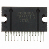
TB6581HG Toshiba, TB6581HG Datasheet

TB6581HG
Specifications of TB6581HG
Available stocks
Related parts for TB6581HG
TB6581HG Summary of contents
Page 1
... Vrefout = 5 V (typ.), 30 mA (max)) • Operating power supply voltage range: V • Motor power supply operating voltage range 50~400 V TB6581HG: TB6581HG is a Pb-free product. The following conditions apply to solderability: *Solderability 1. Use of Sn-37Pb solder bath *solder bath temperature = 230˚C *dipping time = 5 seconds ...
Page 2
Pin Description Pin No. Symbol Description 1 PGND Grounding pin 2 VREG Reference voltage output Connected to pin (typ.), 30 mA (max IGBT emitter pin 4 NC Not connected Signal control power 5 V CC7 ...
Page 3
Pin Assignment PGND IS V Idc CC7 VREG NC Vrefout SGND Absolute Maximum Ratings Characteristics Power supply voltage Input voltage PWM output current Power dissipation Operating temperature Storage temperature Note 1: V ...
Page 4
Recommended operating conditions Characteristics Power supply voltage Crystal oscillator frequency Motor power supply voltage Output current (Ta = 25°C) Symbol Min Typ. Max Unit CC7 V V 13.5 15 16.5 CC15 X ...
Page 5
... CC15 driver VBS undervoltage protection for driver V undervoltage protection for CC7 controller Output turn-on/-off delay time Dead time FRD reverse recovery time Note 6 and Note 7: Toshiba does not implement testing before shipping. Symbol Test Condition = 400 OPEN ...
Page 6
Functional Description 1. Basic operation The motor is driven by the square-wave turn-on signal based on a positional signal. When the positional signal reaches number of rotations higher, the rotor position is estimated according to ...
Page 7
Setting the carrier frequency This function sets the triangular wave cycle (carrier cycle) necessary for generating the PWM signal. (The triangular wave is used for forcibly turning on the lower transistor when the motor is driven by square wave.) ...
Page 8
Monitor protection for V Bootstrap power supply BS When V power supply is lowered, the high-side IGBT is turned off (Output -BS) 9.5 V (typ.) BS High-side IGBT Turn-off high-side IGBT (5) Overheat protection The overheat protection ...
Page 9
Timing Chart • CW (forward) mode (CW mode means that the Hall signal is input in the order shown below Hall signal H v (input signal FG (output) REV signal REV (output) (HIGH ) U ...
Page 10
Example of Application Circuit V refout System clock in generator out Hall Position detector 13 input ...
Page 11
External Parts Symbol Purpose X Internal clock generation Noise absorber oscillation protection 4 refout C 5 Noise absorber ...
Page 12
Package Dimensions Weight: 7.7 g (typ.) 12 TB6581H/HG 2006-03-02 ...
Page 13
... Application Circuits The application circuits shown in this document are provided for reference purposes only. Thorough evaluation is required, especially at the mass production design stage. Toshiba does not grant any license to any industrial property rights by providing these examples of application circuits. 5. Test Circuits Components in the test circuits are used only to obtain and confirm the device characteristics. These components and circuits are not guaranteed to prevent malfunction or failure from occurring in the application equipment ...
Page 14
Points to remember on handling of ICs (1) Over current Protection Circuit Over current protection circuits (referred to as current limiter circuits) do not necessarily protect ICs under all circumstances. If the Over current protection circuits operate against the over ...
Page 15
TB6581H/HG 2006-03-02 ...


