AMIS30542C5421RG ON Semiconductor, AMIS30542C5421RG Datasheet - Page 21
AMIS30542C5421RG
Manufacturer Part Number
AMIS30542C5421RG
Description
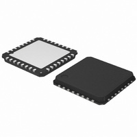
IC MOTOR DVR MICRO STEP 32QFP
Manufacturer
ON Semiconductor
Type
Micro Stepping Motor Driverr
Datasheet
1.AMIS30542C5421RG.pdf
(29 pages)
Specifications of AMIS30542C5421RG
Applications
Stepper Motor Driver, 2 Phase
Number Of Outputs
1
Current - Output
2.2A
Voltage - Supply
6 V ~ 30 V
Operating Temperature
-40°C ~ 125°C
Mounting Type
Surface Mount
Package / Case
32-VSQFP
Product
Stepper Motor Controllers / Drivers
Operating Supply Voltage
6 V to 30 V
Supply Current
8 mA
Mounting Style
SMD/SMT
Lead Free Status / RoHS Status
Lead free / RoHS Compliant
Voltage - Load
-
Lead Free Status / Rohs Status
Lead free / RoHS Compliant
Available stocks
Company
Part Number
Manufacturer
Quantity
Price
Company:

Part Number:
AMIS30542C5421RG
Manufacturer:
ON Semiconductor
Quantity:
1 500
Company:
Part Number:
AMIS30542C5421RG
Manufacturer:
ON Semiconductor
Quantity:
10 000


microcontroller
AMIS−30542. The implemented SPI block is designed to
interface directly with numerous micro−controllers from
several manufacturers. AMIS−30542 acts always as a Slave
and can’t initiate any transmission. The operation of the
device is configured and controlled by means of SPI
registers which are observable for read and/or write from the
Master.
SPI Transfer Format and Pin Signals
(shifted out serially) and received (shifted in serially). A
serial clock line (CLK) synchronizes shifting and sampling
of the information on the two serial data lines (DO and DI).
NOTE:
Transfer Packet:
The transfer packet contains one or more bytes.
Address and indicates to AMIS−30542 the chosen type of
operation and addressed register. Byte 2 contains data, or
The serial peripheral interface (SPI) allows an external
During a SPI transfer, data is simultaneously transmitted
Serial data transfer is assumed to follow MSB first rule.
Byte 1 contains the Command and the SPI Register
At the falling edge of the eight clock pulse the data−out shift register is updated with the content of the addressed internal SPI
register. The internal SPI registers are updated at the first rising edge of the AMIS−30542 system clock when CS = High
CMD2 CMD1 CMD0 ADDR4 ADDR3 ADDR2 ADDR1 ADDR0
MSB
Command
(Master)
Command and SPI Register Address
CLK
# CLK cycle
CS
DO
DI
BYTE 1
to
MSB
MSB
SPI Register Address
communicate
Figure 18. Timing Diagram of a SPI Transfer
1
6
6
Figure 19. SPI Transfer Packet
2
5
5
http://onsemi.com
SPI INTERFACE
3
with
4
4
LSB
4
21
3
3
MSB
DO signal is the output from the Slave (AMIS−30542), and
DI signal is the output from the Master. A chip select line
(CS) allows individual selection of a Slave SPI device in a
multiple−slave system. The CS line is active low. If
AMIS−30542 is not selected, DO is pulled up with the
external pull up resistor. Since AMIS−30542 operates as a
Slave in MODE 0 (CPOL = 0; CPHA = 0) it always clocks
data out on the falling edge and samples data in on rising
edge of clock. The Master SPI port must be configured in
MODE 0 too, to match this operation. The SPI clock idles
low between the transferred bytes.
diagram since CLK, DO and DI pins are directly connected
between the Master and the Slave.
sent from the Master in a WRITE operation, or received
from AMIS−30542 in a READ operation.
D7
5
The diagram below is both a Master and a Slave timing
2
2
D6
6
1
1
D5
7
LSB
LSB
D4
8
Ì Ì Ì Ì
Ì Ì Ì Ì
Ì Ì Ì
Ì Ì Ì
Ì Ì Ì
BYTE 2
Data
D3
D2
D1
LSB
D0
Related parts for AMIS30542C5421RG
Image
Part Number
Description
Manufacturer
Datasheet
Request
R

Part Number:
Description:
ON Semiconductor [VOLTAGE REGULATOR]
Manufacturer:
ON Semiconductor
Datasheet:
Part Number:
Description:
357-036-542-201 CARDEDGE 36POS DL .156 BLK LOPRO
Manufacturer:
ON Semiconductor
Datasheet:
Part Number:
Description:
357-036-542-201 CARDEDGE 36POS DL .156 BLK LOPRO
Manufacturer:
ON Semiconductor
Datasheet:
Part Number:
Description:
357-036-542-201 CARDEDGE 36POS DL .156 BLK LOPRO
Manufacturer:
ON Semiconductor
Datasheet:
Part Number:
Description:
357-036-542-201 CARDEDGE 36POS DL .156 BLK LOPRO
Manufacturer:
ON Semiconductor
Datasheet:
Part Number:
Description:
357-036-542-201 CARDEDGE 36POS DL .156 BLK LOPRO
Manufacturer:
ON Semiconductor
Datasheet:
Part Number:
Description:
357-036-542-201 CARDEDGE 36POS DL .156 BLK LOPRO
Manufacturer:
ON Semiconductor
Datasheet:
Part Number:
Description:
357-036-542-201 CARDEDGE 36POS DL .156 BLK LOPRO
Manufacturer:
ON Semiconductor
Datasheet:
Part Number:
Description:
357-036-542-201 CARDEDGE 36POS DL .156 BLK LOPRO
Manufacturer:
ON Semiconductor
Datasheet:
Part Number:
Description:
357-036-542-201 CARDEDGE 36POS DL .156 BLK LOPRO
Manufacturer:
ON Semiconductor
Datasheet:
Part Number:
Description:
357-036-542-201 CARDEDGE 36POS DL .156 BLK LOPRO
Manufacturer:
ON Semiconductor
Datasheet:
Part Number:
Description:
Manufacturer:
ON Semiconductor
Datasheet:
Part Number:
Description:
Manufacturer:
ON Semiconductor
Datasheet:
Part Number:
Description:
Manufacturer:
ON Semiconductor
Datasheet: