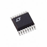
LTC1840CGN Linear Technology, LTC1840CGN Datasheet - Page 7

LTC1840CGN
Manufacturer Part Number
LTC1840CGN
Description
IC DUAL FAN CONTROLLER 16-SSOP
Manufacturer
Linear Technology
Datasheet
1.LTC1840CGN.pdf
(12 pages)
Specifications of LTC1840CGN
Applications
Fan Controller
Number Of Outputs
2
Current - Output
10mA
Voltage - Supply
2.7 V ~ 5.75 V
Operating Temperature
0°C ~ 70°C
Mounting Type
Surface Mount
Package / Case
16-SSOP
Lead Free Status / RoHS Status
Contains lead / RoHS non-compliant
Voltage - Load
-
Available stocks
Company
Part Number
Manufacturer
Quantity
Price
Company:
Part Number:
LTC1840CGN
Manufacturer:
LT
Quantity:
10 000
Part Number:
LTC1840CGN#PBF
Manufacturer:
LINEAR/凌特
Quantity:
20 000
OPERATIO
Serial Interface
The START and STOP Conditions
When the bus is not in use, both SCL and SDA must be
high. A bus master signals the beginning of a transmission
with a START condition by transitioning SDA from high to
low while SCL is high. When the master has finished
communicating with the slave, it issues a STOP condition
by transitioning SDA from low to high while SCL is high.
The bus is then free for another transmission.
Acknowledge
The acknowledge signal is used for handshaking between
the master and the slave. An acknowledge (LOW active)
generated by the slave lets the master know that the latest
byte of information was received. The acknowledge-
related clock pulse is generated by the master. The trans-
mitter master releases the SDA line (HIGH) during the
acknowledge clock pulse. The slave receiver must pull
down the SDA line during the acknowledge clock pulse so
Simple 2-wire interface
Multiple devices on same bus
Idle bus must have SDA and SCL lines high
LTC1840 is read/write
Master controls bus
Devices listen for unique address that precedes data
SDA
SCL
CONDITION
START
S
START 1 1 1 B4 B3 B2 B1
1
U
ADDRESS
1-7
ADDRESS
SLAVE
7
START
1
R/W
WR
8
1
0
1 1 1 B4 B3 B2 B1
ADDRESS
SLAVE
ACK
7
S
1
0
Typical 2-Wire Serial I
ACK
9
X X X X X R2 R1 R0
REGISTER
ADDRESS
WR
1
0
8
LTC1840 Write Byte Protocol
ACK
LTC1840 Read Byte Protocol
S
0
1
1-7
DATA
ACK
X X X X X R2 R1 R0
1
S
0
REGISTER
ADDRESS
START 1 1 1 B4 B3 B2 B1
2
8
1
C or SMBus Transmission
8
that it remains stable LOW during the HIGH period of this
clock pulse.
When a slave receiver doesn’t acknowledge the slave
address (for example, it’s unable to receive because it’s
performing some real-time function), the data line must be
left HIGH by the slave. The master can then generate a
STOP condition to abort the transfer.
If a slave receiver acknowledges the slave address, but
some time later in the transfer cannot receive any more
data bytes, the master must again abort the transfer. This
is indicated by the slave generating the “not acknowledge”
on the first byte to follow. The slave leaves the data line
HIGH and the master generates the STOP condition.
Commands Supported
The LTC1840 supports read byte, write byte, read word
(the second data byte will be all ones) and write word (the
second data byte will be ignored) commands.
Data Transfer Timing for Write Commands
In order to help assure that bad data is not written into the
LTC1840, data from a write command is only stored after
a valid acknowledge has been performed. The part will
detect that SDA is low on the rising edge of SCL that marks
the end of the period in which the LTC1840 acknowledges
the data write and then latch the data during the following
SCL low period.
ADDRESS
SLAVE
ACK
S
7
1
0
ACK
9
D7 D6 D5 D4 D3 D2 D1 D0
RD
1
1
DATA
BYTE
8
ACK
1-7
1
S
0
DATA
D7 D6 D5 D4 D3 D2 D1 D0
ACK
S
1
0
DATA
BYTE
8
8
STOP
1
ACK
9
ACK
M
1
1
LTC1840
CONDITION
STOP
1840 TD03
1
STOP
P
1840 TD02
7
1840f


