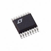
LTC1840CGN Linear Technology, LTC1840CGN Datasheet - Page 5

LTC1840CGN
Manufacturer Part Number
LTC1840CGN
Description
IC DUAL FAN CONTROLLER 16-SSOP
Manufacturer
Linear Technology
Datasheet
1.LTC1840CGN.pdf
(12 pages)
Specifications of LTC1840CGN
Applications
Fan Controller
Number Of Outputs
2
Current - Output
10mA
Voltage - Supply
2.7 V ~ 5.75 V
Operating Temperature
0°C ~ 70°C
Mounting Type
Surface Mount
Package / Case
16-SSOP
Lead Free Status / RoHS Status
Contains lead / RoHS non-compliant
Voltage - Load
-
Available stocks
Company
Part Number
Manufacturer
Quantity
Price
Company:
Part Number:
LTC1840CGN
Manufacturer:
LT
Quantity:
10 000
Part Number:
LTC1840CGN#PBF
Manufacturer:
LINEAR/凌特
Quantity:
20 000
SCL (Pin 1): Serial Clock Input. The 2-wire bus master
device clocks this pin at a frequency between 0kHz and
100kHz to enable serial bus communications. Data at the
SDA pin is shifted in or out on rising SCL edges. SCL has
a logic threshold of 1V and an external pull-up resistor or
current source is normally required.
SDA (Pin 2): Serial Data Input. This is a bidirectional data
pin which normally has an external pull-up resistor or
current source and can be pulled down by the open drain
device on the LTC1840 or by external devices. The master
controls SDA during addressing, the writing of data, and
read acknowledgment, while the LTC1840 controls SDA
when data is being read back and during write acknowl-
edgment. SDA data is shifted in or out on rising SCL edges.
SDA has a logic threshold of 1V.
A1 (Pin 3): Three State Address Programming Input. This
pin can cause three different logic states internally, de-
pending upon whether it is pulled to supply, pulled to
ground, or not connected (NC). Combined with the A0 pin,
this provides for nine different possible two-wire bus
addresses for the LTC1840 (see Table 1).
A0 (Pin 4): Three State Address Programming Input. See
A1.
FAULT (Pin 5): Fault Indicator Pull-Down Output. This pin
has an open drain pull-down that is used to signal various
TYPICAL PERFOR A CE CHARACTERISTICS
PI FU CTIO S
U
U
–0.1
–0.2
0.4
0.3
0.2
0.1
0
0
DAC INL at V
T
U
A
= 25 C
W
CC
CODE
= 3V
U
1840 G10
255
fault conditions on the LTC1840. An external 10k pull-up
is recommended.
GPIO1, GPIO2, GPIO3, GPIO4 (Pins 6, 7, 9, 10): General
Purpose Inputs/Outputs. These pins can be used as digital
inputs with CMOS logic thresholds or digital outputs/LED
drivers with open drain pull-downs that can be pro-
grammed to blink. GPIO pins can be programmed to
produce faults due to changes in their logic states, and
these faults can only be cleared by software or powering
the LTC1840 down. All GPIOs default to nonfaulting logic
inputs upon power-up and their functionality is changed
through the serial interface.
GND (Pin 8): Ground. Connect to analog ground plane.
TACHA (Pin 11): Tachometer Input A. This pin is a digital
input that is designed to interface to the tachometer output
from a 3-wire fan. Internal logic counts between rising
TACHA edges at serially programmable frequencies of
25kHz, 12.5kHz, 6.25kHz or 3.125kHz and the most re-
cently completed count is stored in a register accessible
through the serial interface. The maximum count is 255
and the LTC1840 is programmable to produce faults when
a count exceeds this number. This pin has CMOS thresh-
olds and the default conditions are to count at 3.125kHz
and to not produce faults.
TACHB (Pin 12): Tachometer Input B. See TACHA
1.011
1.010
1.009
1.008
1.007
1.006
1.005
1.004
1.003
1.002
–50
BLAST Falling Threshold
at V
CC
–25
= 3V
TEMPERATURE ( C)
0
25
50
75
1840 G11
LTC1840
100
5
1840f


