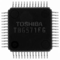
TB6571FG(O,EL) Toshiba, TB6571FG(O,EL) Datasheet - Page 11

TB6571FG(O,EL)
Manufacturer Part Number
TB6571FG(O,EL)
Description
IC DC MOTOR CTRLR BRUSHLSS 52QFP
Manufacturer
Toshiba
Specifications of TB6571FG(O,EL)
Applications
DC Motor Controller, Brushless (BLDC), 3 Phase
Number Of Outputs
1
Voltage - Supply
10 V ~ 28 V
Operating Temperature
-30°C ~ 85°C
Mounting Type
Surface Mount
Package / Case
52-QFP
Mounting Style
SMD/SMT
Lead Free Status / RoHS Status
Lead free / RoHS Compliant
Current - Output
-
Voltage - Load
-
Lead Free Status / Rohs Status
Lead free / RoHS Compliant
Other names
TB6571FGTR
Available stocks
Company
Part Number
Manufacturer
Quantity
Price
(Note)
External FET Gate Drive Output
Speed Control
Fref signal
• The TB6571FG uses a speed discriminator and PLL to control speed.
• The speed discriminator has two counter stages, each of which alternately counts a single period of the FG
• The PLL counts the phase difference between the 1/2 FG signal and reference signal. The resulting
• The gain ratio between the speed discriminator and PLL is set using an external resistor.
• The total gain is set using an external constant for the charge pump.
• VCO PLL
• FG frequency = speed control clock/speed discriminator
• When the Fref input is open, the output is turned off.
• Note that a sudden variation in rotation speed may cause a motor current to be regenerated into the power
• When the system clock is saturated, a READY signal may remain being L output even if external clock
FG signal
The output for driving the upper FET is divided into two pins
so that resistor adjustment is enabled only for gate driving
The output for driving the lower FET is also divided.
The upper FET is driven with the LA(U1) pin on the source
and the LA(U2) pin on the sink. The lower FET is driven with
signal. The resulting difference signal is output as two signals (charge pulses and discharge pulses).
difference signal is output as two signals (charge pulses and discharge pulses). The phase difference is
assumed to be zero when the FG frequency is outside the lock range (±6% of the specified value).
The maximum guaranteed range for the VCO oscillation frequency is a quadruple width, with a single
external constant as a condition.
→ Speed control clock = FG frequency × speed discriminator
supply, resulting in the rise of the motor voltage.
frequency and FG frequency shift. Please confirm optimization of a VCO system PLL circuit
constant(25pin,22pin).
(sourcing), thus reducing impedance for extraction.
LA(L1) on the source and LA(L2) on the sink.
comparator
FG frequency = 200 to 2 k, speed discriminator = 1024
Speed control clock = 0.2048 to 2.048 MHz
System clock = speed control clock × 4
Phase
frequency
amplifier
1/1024
divider
= 0.8192 to 8.192 MHz
FG
LPF
frequency
divider
1/4
VCO
discriminator
11
Speed
1024
PLL
Sine wave system clock
5V
Charge
pump
LA(U1)
LA(U2)
OUT-A
LA(L1)
LA(L2)
PLL-Gain
CP
amplifier
Control
Upper FET
Lower FET
TB6571FG
2005-04-15


