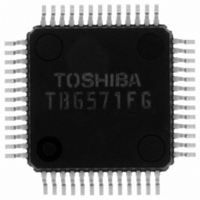
TB6571FG(O,EL) Toshiba, TB6571FG(O,EL) Datasheet

TB6571FG(O,EL)
Specifications of TB6571FG(O,EL)
Available stocks
Related parts for TB6571FG(O,EL)
TB6571FG(O,EL) Summary of contents
Page 1
... TOSHIBA Bi-CMOS Integrated Circuit Silicon Monolithic 3-Phase Full-Wave Brushless Motor Controller Featuring Speed Control and Sine Wave PWM Drive The TB6571FG is a 3-phase full-wave brushless motor controller IC that employs a sine wave PWM drive mechanism with a speed control function. Sine wave current driving with 2-phase modulation enables the IC to drive a motor with high efficiency and low noise ...
Page 2
Block Diagram Some of the functional blocks, circuits, or constants in the block diagram may be omitted or simplified for explanatory purpose. R22 C19 C18 C17 Fref LP1 15 25 Phase comparator LPF 1/N frequency divider HA+ ...
Page 3
Pin Functions Pin No. Name 1 LC (L1) Phase-C energization signal output (L1 connection 3 HA+ Phase-A hall signal input + pin 4 HA− Phase-A hall signal input - pin 5 HB+ Phase-B hall signal input + ...
Page 4
Pin No. Name 41 OUT-A Phase-A motor pin 42 LA (L2) Phase-A energization signal output (L2 (L1) Phase-A energization signal output (L1 (U1) Phase-B energization signal output (U1 (U2) Phase-B energization signal output (U2) ...
Page 5
Maximum Ratings Characteristics Supply voltage Input voltage Output voltage Output current Power dissipation Operating temperature Storage temperature Note 1: CW/CCW, STB,START,BRAKE, Idc,Fref Note 2: Ready, FGS Note 3: LA (U), LB (U), LC (U) Note 4: LA ...
Page 6
Functional Description The equivalent circuit diagrams may be simplified or some parts of them may be omitted for explanatory purpose. Sine Wave PWM Drive <Energization Switching> Upon start-up, the TB6571FG drives the motor with square waves for 120° energization using ...
Page 7
The TB6571FG uses position detection signals to create modulation waveforms, which it compares with triangular waves to generate sine wave PWM signals. It counts the time between zero-crossing points for the three position detection signals (electrical angle: 60°) and uses ...
Page 8
In addition, the TB6571FG performs phase alignment with the modulation waveforms at each zero-crossing in the position detection signals. For every 60° of electrical angle, it synchronizes with the rising and falling edges of the position detection signals (Hall amplifier ...
Page 9
Timing Charts HA Position detection HB (Hall amplifier HC output) LA (U) Energization LB (U) signal output LC (U) when driven LA (L) with square wave LB ( Modulation waveform when driven with sine S B ...
Page 10
Generating an Internal Reference Clock The TB6571FG uses external C and R to generate a reference clock internally. It uses the reference clock to generate triangular waves, which determine the carrier frequency, and set a dead time. The clock also ...
Page 11
External FET Gate Drive Output The output for driving the upper FET is divided into two pins so that resistor adjustment is enabled only for gate driving (sourcing), thus reducing impedance for extraction. The output for driving the lower FET ...
Page 12
Charge Pump control amplifier I1 • The charge pump consists of MOS transistors, which enable fast switching, thus allowing control with higher resolution. For the speed discriminator and PLL gains, the ratio of the charge/discharge ...
Page 13
Control amplifier CP • The voltage integrated in the charge pump is input to the control amplifier. The input is placed in high-impedance state because P-ch gate. • The control amplifier circuit has an offset of 0.45 ...
Page 14
FG amplifier/hysteresis comparator V ref FGin • The FG amplifier supports pattern FG and incorporates an internal reference voltage of 2.5 V. Entering a sine wave of 50 mVpp or greater results in a signal multiplied by ...
Page 15
Hall amplifier + HA • The Hall amplifier accepts Hall device output signals. If input signals contain noise, connect a capacitor between inputs. • The common-mode input voltage range is: VCMRH = 1.5 to 3.5 V. The Hall amplifier has ...
Page 16
Forward/reverse rotation circuit CW/CCW The circuit accepts a TTL input and incorporates a pull-up resistor. CW/CCW Input Mode H Reverse L Forwared + → Forward: Hall device signals Note that abrupt switching between forward and reverse rotation may ...
Page 17
Operation sequence VM power supply Vref power supply (+ power DD supply (+ power supply (+8 V) Internal reference clock fx2 Output charge pump voltage External reference clock fref System clock fx1 (fref multiplied) PLL lockup ...
Page 18
Automatic phase lead angle correction circuit ・ The circuit corrects the lead angle using the motor current value. Automatic lead angle correction Motor current VRF RF R2 *)Gain = (R2+R3 VRF V [ • The circuit can advance ...
Page 19
Constant voltage circuit (1) Vref1 • The circuit creates 5 V for biasing the internal analog circuit and outputs it from the Vref pin. Connect a capacitor (0.1 µ µF) between the Vref pin and L-GND to prevent ...
Page 20
Electrical characteristics Characteristics Supply current Common-mode input voltage range Hall Input amplitude range amplifier Input hysteresis Input current Remaining output voltage Ready circuit Output leakage current Input offset voltage Remaining output voltage (upper) FG Remaining output voltage amplifier (lower) Reference ...
Page 21
Characteristics Rising voltage Control Saturation voltage amplifier Input current Charge current Charge pump Discharge current Reference clock Lock frequency protection circuit Operating time Test Symbol Test conditions Circuit VCR VCLP IinCP (source current), Vcp = 3.1 V, Icp + V(PLL-GAIN)=0V ...
Page 22
Package Dimensions Weight: 0.0 g (typ.) 22 TB6571FG 2005-04-15 ...
Page 23
... The information contained herein is presented only as a guide for the applications of our products. No responsibility is assumed by TOSHIBA for any infringements of patents or other rights of the third parties which may result from its use. No license is granted by implication or otherwise under any patent or patent rights of TOSHIBA or others. • ...


