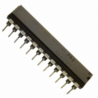
L6235N STMicroelectronics, L6235N Datasheet - Page 16

L6235N
Manufacturer Part Number
L6235N
Description
IC DRIVER 3PHASE MOTOR 24-PWRDIP
Manufacturer
STMicroelectronics
Type
Driverr
Datasheet
1.L6235D013TR.pdf
(25 pages)
Specifications of L6235N
Applications
DC Motor Driver, Brushless (BLDC), 3 Phase
Number Of Outputs
1
Current - Output
5.6A
Voltage - Supply
12 V ~ 52 V
Operating Temperature
-25°C ~ 125°C
Mounting Type
Through Hole
Package / Case
24-DIP (0.300", 7.62mm)
Operating Supply Voltage
7 V to 52 V
Supply Current
0.006 A
Mounting Style
Through Hole
Motor Type
Three Phase DC Brushless
No. Of Outputs
3
Output Current
7.1A
Output Voltage
52V
Supply Voltage Range
8V To 52V
Driver Case Style
DIP
No. Of Pins
24
Rohs Compliant
Yes
For Use With
497-4935 - BOARD MOTOR BRUSHLESS DC L6235
Lead Free Status / RoHS Status
Lead free / RoHS Compliant
Voltage - Load
-
Lead Free Status / Rohs Status
Lead free / RoHS Compliant
Other names
497-5353-5
L6235N
L6235N
L6235
NON-DISSIPATIVE OVERCURRENT DETECTION and PROTECTION
The L6235 integrates an Overcurrent Detection Circuit (OCD) for full protection. This circuit provides Output-to-
Output and Output-to-Ground short circuit protection as well. With this internal over current detection, the exter-
nal current sense resistor normally used and its associated power dissipation are eliminated. Figure 17 shows
a simplified schematic for the overcurrent detection circuit.
To implement the over current detection, a sensing element that delivers a small but precise fraction of the out-
put current is implemented with each High Side power MOS. Since this current is a small fraction of the output
current there is very little additional power dissipation. This current is compared with an internal reference cur-
rent I
ator signals a fault condition. When a fault condition is detected, an internal open drain MOS with a pull down
capability of 4mA connected to pin DIAG is turned on.
The pin DIAG can be used to signal the fault condition to a C or to shut down the Three-Phase Bridge simply
by connecting it to pin EN and adding an external R-C (see R
Figure 17. Overcurrent Protection Simplified Schematic
Figure 18 shows the Overcurrent Detetection operation. The Disable Time t
operation can be easily programmed by means of the accurate thresholds of the logic inputs. It is affected
whether by C
ing off the bridge when an overcurrent has been detected depends only by C
in Figure 20.
C
should be chosen as big as possible according to the maximum tolerable Delay Time and the R
be chosen according to the desired Disable Time.
The resistor R
are respectively 100K
16/25
EN
is also used for providing immunity to pin EN against fast transient noises. Therefore the value of C
REF
C or LOGIC
V
DD
. When the output current reaches the detection threshold (typically I
R
C
EN
EN
EN
EN
and R
should be chosen in the range from 2.2K to 180K . Recommended values for R
DIAG
EN
EN
and 5.6nF that allow obtaining 200 s Disable Time.
TO GATE
40 TYP.
values and its magnitude is reported in Figure 19. The Delay Time t
R
LOGIC
DS(ON)
POWER SENSE
OPEN-DRAIN
INTERNAL
1 cell
COMPARATOR
OCD
HIGH SIDE DMOS
POWER DMOS
OVER TEMPERATURE
n cells
I
1
OUT
I
1
/ n
1
I
I
I
REF
REF
1
+I
VS
2
+
/ n
A
OUT
I
2
EN
/ n
2
POWER DMOS
HIGH SIDE DMOS
I
2
, C
n cells
EN
).
D02IN1381
POWER SENSE
I
3
EN
1 cell
/ n
DISABLE
SOVER
value. Its magnitude is reported
OUT
= 5.6A) the OCD compar-
3
POWER DMOS
before recovering normal
I
3
VS
n cells
B
HIGH SIDE DMOS
DELAY
EN
POWER SENSE
value should
before turn-
EN
1 cell
and C
EN
EN


