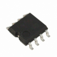
BD6210F-E2 Rohm Semiconductor, BD6210F-E2 Datasheet - Page 8

BD6210F-E2
Manufacturer Part Number
BD6210F-E2
Description
IC H-BRIDGE DVR 7V 1CH .5A 8-SOP
Manufacturer
Rohm Semiconductor
Specifications of BD6210F-E2
Applications
DC Motor Driver
Number Of Outputs
1
Current - Output
500mA
Voltage - Supply
3 V ~ 5.5 V
Operating Temperature
-40°C ~ 85°C
Mounting Type
Surface Mount
Package / Case
8-SOP
No. Of Outputs
1
Output Current
500mA
Supply Voltage Range
3V To 5.5V
Driver Case Style
SOP
No. Of Pins
8
Operating Temperature Range
-40°C To +85°C
Svhc
No SVHC (18-Jun-2010)
Package /
RoHS Compliant
Product
H-Bridge Drivers
Supply Voltage (max)
7 V
Supply Voltage (min)
3 V
Supply Current
0.7 mA
Maximum Power Dissipation
0.687 W
Maximum Operating Temperature
+ 85 C
Mounting Style
SMD/SMT
Bridge Type
H-bridge
Minimum Operating Temperature
- 40 C
Number Of Drivers
1
Operating Supply Voltage
3 V to 5.5 V
Motor Type
H-Bridge
Rohs Compliant
Yes
Base Number
6210
Lead Free Status / RoHS Status
Lead free / RoHS Compliant
Voltage - Load
-
Lead Free Status / Rohs Status
Lead free / RoHS Compliant
Other names
BD6210F-E2TR
Available stocks
Company
Part Number
Manufacturer
Quantity
Price
Company:
Part Number:
BD6210F-E2
Manufacturer:
ROHM Semiconductor
Quantity:
2 001
Company:
Part Number:
BD6210F-E2
Manufacturer:
ROHM
Quantity:
2 642
Company:
Part Number:
BD6210F-E2
Manufacturer:
ROHM
Quantity:
32
Part Number:
BD6210F-E2
Manufacturer:
ROHM/罗姆
Quantity:
20 000
Block diagram and pin configuration - Continued
○
BD6210, BD6211, BD6212, BD6215, BD6216, BD6217
c
www.rohm.com
BD6217FM
2009 ROHM Co., Ltd. All rights reserved.
VREFA
VREFB
RINA
RINB
FINA
GND
FINB
GND
11
10
22
23
25
24
9
8
OUT1A
OUT1A
OUT2A
OUT2A
VREFA
RNFA
RNFA
RINA
FINA
GND
GND
VCC
VCC
VCC
NC
Fig.36 HSOP-M28
Fig.35 BD6217FM
DUTY
DUTY
CTRL
CTRL
PROTECT
PROTECT
GND
FIN
VCC
VCC
VCC
FINB
RINB
VREFB
GND
GND
OUT2B
OUT2B
NC
RNFB
RNFB
OUT1B
OUT1B
26
27
28
12
13
14
15
16
20
21
17
18
1
2
6
7
3
4
VCC
VCC
OUT1A
OUT2A
RNFA
VCC
VCC
OUT1B
OUT2B
RNFB
8/16
Note: All pins not described above are NC pins.
Note:
13,14
15,16
17,18
20,21
27,28
FIN
Pin
1,2
3,4
6,7
10
11
12
22
23
24
25
26
8
9
Use all VCC pin by the same voltage.
OUT1A
OUT2A
VREFA
OUT1B
OUT2B
VREFB
RNF A
RNFB
Name
RINA
RINB
GND
FINA
GND
FINB
GND
VCC
VCC
VCC
VCC
Table 6 BD6217FM
Driver output
Power stage ground
Driver output
Small signal ground
Duty setting pin
Control input (reverse)
Control input (forward)
Power supply
Power supply
Driver output
Power stage ground
Driver output
Small signal ground
Duty setting pin
Control input (reverse)
Control input (forward)
Power supply
Power supply
Ground
Function
2009.08 - Rev.C
Technical Note


