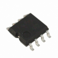
BD6210F-E2 Rohm Semiconductor, BD6210F-E2 Datasheet

BD6210F-E2
Specifications of BD6210F-E2
Available stocks
Related parts for BD6210F-E2
BD6210F-E2 Summary of contents
Page 1
TECHNICAL NOTE For brush motors H-bridge drivers (7V max.) BD6210, BD6211, BD6212, BD6215, BD6216, BD6217 Overview These H-bridge drivers are full bridge drivers for brush motor applications. Each IC can operate at a wide range of power-supply voltages (from 3V ...
Page 2
Absolute maximum ratings (Ta=25°C) Parameter Supply voltage Output current All other input pins Operating temperature Storage temperature Power dissipation Junction temperature *** Notes: All voltages are with respect to ground. *1 BD6210 / BD6215. Do not, exceed Pd or ASO. ...
Page 3
Electrical characteristic curves (Reference data) 1.0 85°C 25°C 0.8 -40°C 0.6 0.4 0.2 0 Supply Voltage: Vcc [V] Fig.1 Supply current 100 80 85°C 25°C -40° Input ...
Page 4
Electrical characteristic curves (Reference data) – Continued 0.4 85°C 25°C -40°C 0.3 0.2 0 0.1 0.2 0.3 0.4 0.5 Output Current: I [A] OUT Fig.13 Output high voltage (0.5A class) 2 -40°C 25°C 85°C 1.5 1 0.5 0 ...
Page 5
... Block diagram and pin configuration BD6210F / BD6211F VREF 6 DUTY PROTECT FIN 4 CTRL RIN 5 1 OUT1 Fig.25 BD6210F / BD6211F OUT1 GND VCC OUT2 VCC VREF FIN RIN Fig.26 SOP8 BD6210HFP / BD6211HFP / BD6212HFP VREF DUTY PROTECT 1 FIN 3 CTRL RIN 5 FIN 2 GND OUT1 Fig.27 BD6210/11/12HFP Fig ...
Page 6
Block diagram and pin configuration – Continued BD6212FP VREF DUTY PROTECT 17 FIN 20 CTRL RIN 19 6 FIN 1 2 GND GND OUT1 Fig.29 BD6212FP OUT1 NC OUT1 NC NC VCC NC VCC NC VCC GND FIN GND GND ...
Page 7
Block diagram and pin configuration – Continued BD6215FP, BD6216FP/FM VREFA DUTY PROTECT 9 FINA 11 CTRL RINA 10 GND 20 VREFB 21 DUTY PROTECT FINB 23 CTRL RINB 22 GND 8 FIN GND Fig. 33 BD6215FP, BD6216FP OUT1A VCC NC ...
Page 8
Block diagram and pin configuration – Continued BD6217FM VREFA DUTY PROTECT 9 FINA 11 CTRL RINA 10 GND 22 VREFB 23 DUTY PROTECT FINB 25 CTRL RINB 24 GND 8 FIN GND Fig. 36 BD6217FM OUT1A OUT1A RNFA RNFA NC ...
Page 9
Functional descriptions 1) Operation modes FIN RIN PWM PWM Hi-Z is the off state of all output ...
Page 10
PWM control mode The rotational speed of the motor can be controlled by the switching duty when the PWM signal is input to the FIN pin or the RIN pin. In this mode, the high side output is ...
Page 11
Cross-conduction protection circuit In the full bridge output stage, when the upper and lower transistors are turned on at the same time, and this condition exists during the period of transition from high to low, or low to high, ...
Page 12
Thermal design 1.5 i) Package only ii) Mounted on ROHM standard PCB (70mm x 70mm x 1.6mm FR4 glass -epoxy board) 1.0 ii) 0.687W 0.5 i) 0.562W 0 100 125 AMBIENT TEMPERATURE [°C] Fig.43 Thermal derating ...
Page 13
Interfaces VCC 100k FIN VREF RIN 100k Fig.48 FIN / RIN NOTES FOR USE 1) Absolute maximum ratings Devices may be destroyed when supply voltage or operating temperature exceeds the absolute maximum rating. Because the cause of this damage cannot ...
Page 14
ASO - Area of Safety Operation When using the IC, set the output transistor so that it does not exceed absolute maximum ratings or ASO. 9) Built-in thermal shutdown (TSD) circuit The TSD circuit is designed only to shut ...
Page 15
SOP8 SOP8 <Dimension> <Dimension> 5.0±0.2 5.0±0 0.15±0.1 0.15±0.1 0.1 0.1 1.27 1.27 0.4±0.1 0.4±0.1 (Unit:mm) (Unit:mm) SSOP-B24 <Dimension> 7.8 ± 0 0.15 ± 0.1 0.1 0.65 0.22 ± ...
Page 16
HRP7 <Dimension> 9.395 ± 0.125 (MAX 9.745 include BURR) 1.905 ± 0.1 8.82 – 0.1 (5.59 0.8875 + 5.5 4.5 - 4.5 + 0.1 0.27 - 0.05 S 0.73 ± 0.1 1.27 0.08 ...
Page 17
Appendix No technical content pages of this document may be reproduced in any form or transmitted by any means without prior permission of ROHM CO.,LTD. The contents described herein are subject to change without notice. The specifications for the product ...


