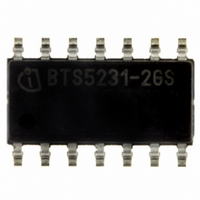
BTS5231-2GS Infineon Technologies, BTS5231-2GS Datasheet - Page 14

BTS5231-2GS
Manufacturer Part Number
BTS5231-2GS
Description
IC PWR SWITCH HISIDE PGDSO-14-31
Manufacturer
Infineon Technologies
Series
PROFET®r
Type
High Sider
Datasheet
1.BTS5231-2GS.pdf
(27 pages)
Specifications of BTS5231-2GS
Package / Case
DSO-14
Input Type
Non-Inverting
Number Of Outputs
2
On-state Resistance
140 mOhm
Current - Output / Channel
1.8A
Current - Peak Output
10A
Voltage - Supply
4.5 V ~ 28 V
Operating Temperature
-40°C ~ 150°C
Mounting Type
Surface Mount
On Resistance (max)
140 mOhms
Maximum Operating Temperature
+ 150 C
Minimum Operating Temperature
- 40 C
Maximum Power Dissipation
900 mW
Mounting Style
SMD/SMT
Supply Current
3.8 mA
Power Load Switch Type
High Side
Input Voltage
28V
Current Limit
8A
On State Resistance
0.14ohm
Thermal Protection
ESD
Power Dissipation Pd
900mW
No. Of Outputs
2
Internal Switch
No
Rohs Compliant
Yes
Distribution Switch Case Style
SOIC
Lead Free Status / RoHS Status
Lead free / RoHS Compliant
Lead Free Status / RoHS Status
Lead free / RoHS Compliant, Lead free / RoHS Compliant
Other names
BTS5231-2GSINTR
BTS52312GSXT
SP000281794
BTS52312GSXT
SP000281794
Available stocks
Company
Part Number
Manufacturer
Quantity
Price
Part Number:
BTS5231-2GS
Manufacturer:
INFINEON/英飞凌
Quantity:
20 000
V
typical values:
Pos.
Thermal Resistance
4.1.10 Junction to case
4.1.11 Junction to ambient
Input Characteristics
4.1.12 Input resistance
4.1.13 L-input level
4.1.14 H-input level
4.1.15 Input hysteresis
4.1.16 L-input current
4.1.17 H-input current
Timings
4.1.18 Turn-on time to
4.1.19 Turn-off time to
4.1.20 slew rate
4.1.21 slew rate
1) Not subject to production test, specified by design
2) Device mounted on PCB (50 mm × 50 mm × 1.5 mm epoxy, FR4) with 6 cm
3) Not subject to production test, parameters are calculated from
Note: Characteristics show the deviation of parameter at the given supply voltage and
Data Sheet
bb
layer, 70 µm thick) for
= 9 V to 16 V,
junction temperature. Typical values show the typical parameters expected from
manufacturing.
Parameter
one channel active
all channels active
90%
10%
30% to 70%
70% to 30%
V
V
OUT
OUT
V
bb
T
= 13.5 V,
j
V
V
V
= -40 °C to +150 °C (unless otherwise specified)
bb
OUT
OUT
connection. PCB is vertical without blown air
2)
T
j
= 25 °C
Symbol
R
R
R
V
V
∆
I
I
t
t
d
-d
d
ON
OFF
IN(L)
IN(H)
V
t
V
thjc
thja
IN
IN(L)
IN(H)
OFF
V
/ d
IN
/
Block Description and Electrical Characteristics
t
ON
min.
-0.3
2.0
2.6
0.1
0.1
14
10
3
Limit Values
0.25
0.26
typ. max.
100
3.5
0.3
75
71
18
38
80
Smart High-Side Power Switch
R
DS(ON)
250 µs
250 µs
5.5
1.0
5.7
0.5
0.5
48
75
75
and
R
Unit
K/W
K/W
kΩ
V
V
V
µA
µA
V/µs
V/µs
th
2
copper heatsinking area (one
Test Conditions
1)
1) 2)
1)
V
V
R
V
R
V
R
V
R
V
IN
IN
L
bb
L
bb
L
bb
L
bb
BTS5231-2GS
V1.1, 2007-06-14
= 12 Ω,
= 12 Ω,
= 12 Ω,
= 12 Ω,
= 0.4 V
= 5 V
= 13.5 V
= 13.5 V
= 13.5 V
= 13.5 V


