VND05B-E STMicroelectronics, VND05B-E Datasheet
VND05B-E
Specifications of VND05B-E
Available stocks


Related parts for VND05B-E


VND05B-E Summary of contents
Page 1
... THERMAL SHUT-DOWN UNDERVOLTAGE PROTECTION OPEN DRAIN DIAGNOSTIC OUTPUT INDUCTIVE LOAD FAST DEMAGNETIZATION VERY LOW STAND-BY POWER DISSIPATION DESCRIPTION The VND05B, VND05B (011Y), VND05B (012Y monolithic device STMicroelectronics VIPower technology, intended for driving resistive or inductive loads with one side connected to ground. This device has two channels, and a common diagnostic ...
Page 2
... VND05B / VND05B (011Y) / VND05B (012Y) ABSOLUTE MAXIMUM RATING Symbol V Drain-Source breakdown voltage (BR)DSS I Output current (continuous OUT I (RMS) RMS Output current at T OUT I Reverse output current Input current IN -V Reverse supply voltage CC I Status current STAT V Electrostatic discharge (R=1.5k , C=100pF) ESD ...
Page 3
... Parameter V Input low level voltage IL V Input high level voltage IH V Input hysteresis voltage I(hyst) I Input current IN V Input clamp voltage ICL VND05B / VND05B (011Y) / VND05B (012Y) Parameter (MAX) (MAX) <16V; -40 T 125 °C ° Test Conditions T =85°C; V 0.5V; V =13V ...
Page 4
... VND05B / VND05B (011Y) / VND05B (012Y) ELECTRICAL CHARACTERISTICS (continued) PROTECTIONS AND DIAGNOSTICS Symbol Parameter V Low output voltage status I STAT V Undervoltage shut-down USD Status clamp voltage V SCL Thermal shut-down T TSD temperature Thermal shutdown T TSD(hyst) hysteresis temperature T Reset temperature R V Open voltage level OL I Open load current level ...
Page 5
... CC where f= switching frequency and V = demagnetization voltage. demag VND05B / VND05B (011Y) / VND05B (012Y) The maximum inductance which causes the chip temperature to reach the shutdown temperature in a specified thermal environment is a function of the load current for a fixed V according to the above formula. In this device if the GND pin is disconnected, with V 16V, both channels will switch off ...
Page 6
... VND05B / VND05B (011Y) / VND05B (012Y) THRUTH TABLE Normal operation Undervoltage Channel 1 Thermal shutdown Channel 2 Channel 1 Openload Channel 2 Channel 1 Output shorted Channel 2 Figure: 1: Waveforms 6/11 1 INPUT 1 INPUT 2 OUTPUT OUTPUT 2 DIAGNOSTIC ...
Page 7
... Figure 2: Typical application circuit with a Schottky diode for reverse supply protection Figure 3: Typical application circuit with separate signal ground VND05B / VND05B (011Y) / VND05B (012Y) 7/11 2 ...
Page 8
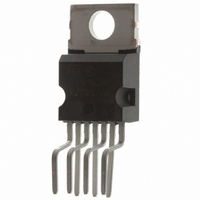
... VND05B / VND05B (011Y) / VND05B (012Y) HEPTAWATT (horizontal) MECHANICAL DATA DIM. MIN 2.4 D1 1.2 E 0. 2.41 G1 4. 10. 2 Dia 3.65 8/ mm. TYP MAX. MIN. 4.8 1.37 2.8 0.094 1.35 0.047 0.55 0.014 0.8 0.024 0.9 2.54 2.67 0.095 5.08 5 ...
Page 9
... D1 1.2 E 0. 2.41 G1 4. 10. 2 VND05B / VND05B (011Y) / VND05B (012Y) mm. TYP MAX. MIN. 4.8 1.37 2.8 0.094 1.35 0.047 0.55 0.014 0.8 0.024 0.9 2.54 2.67 0.095 5.08 5.21 0.193 7.62 7.8 0.295 10.4 10.4 0.396 16.97 14.92 21 ...
Page 10
... VND05B / VND05B (011Y) / VND05B (012Y) HEPTAWATT (in-line) MECHANICAL DATA DIM. MIN 2.4 D1 1.2 E 0. 2.41 G1 4. 10.05 L2 22.4 L3 25.4 L5 2 Dia. 3.65 10/ mm. TYP MAX. MIN. 4.8 1.37 0.094 2.8 1.35 0.047 0.55 0.014 0.8 0.024 0.9 2.54 2 ...
Page 11
... STMicroelectronics - Printed in ITALY- All Rights Reserved. Australia - Brazil - Canada - China - France - Germany - Italy - Japan - Korea - Malaysia - Malta - Mexico - Morocco - The Netherlands - Singapore - Spain - Sweden - Switzerland - Taiwan - Thailand - United Kingdom - U.S.A. VND05B / VND05B (011Y) / VND05B (012Y) The ST logo is a trademark of STMicroelectronics STMicroelectronics GROUP OF COMPANIES http://www ...