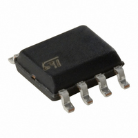
VNS3NV04D STMicroelectronics, VNS3NV04D Datasheet

VNS3NV04D
Specifications of VNS3NV04D
497-2668-5
497-3318-5
Available stocks
Related parts for VNS3NV04D
VNS3NV04D Summary of contents
Page 1
... POWER MOSFET (ANALOG DRIVING) n COMPATIBLE WITH STANDARD POWER MOSFET DESCRIPTION The VNS3NV04D is a device formed by two monolithic OMNIFET II chips housed in a standard SO-8 package. The OMNIFET II are designed in STMicroelectronics VIPower M0-3 Technology: they are intended for replacement of standard Power MOSFETS from 50KHz ...
Page 2
... VNS3NV04D ABSOLUTE MAXIMUM RATING Symbol V Drain-source Voltage (V DSn V Input Voltage INn I Input Current INn R Minimum Input Series Impedance IN MINn I Drain Current Dn I Reverse DC Output Current Rn V Electrostatic Discharge (R=1.5K , C=100pF) ESD1 V Electrostatic Discharge on output pins only (R=330 , C=150pF) ESD2 P Total Dissipation at T ...
Page 3
... I =1mA =0V =1mA IN I =-1mA IN V =13V; V =0V; T =25° =25V Test Conditions V =5V; I =1.5A; T =25° =5V; I =1. VNS3NV04D Value Unit 30 °C/W 80(*) °C/W Min Typ Max Unit 0.5 2.5 V 100 150 -1.0 -0 Min Typ Max Unit 120 m 240 3/14 1 ...
Page 4
... VNS3NV04D ELECTRICAL CHARACTERISTICS (continued) (T DYNAMIC Symbol Parameter Forward g (*) fs Transconductance C Output Capacitance OSS SWITCHING Symbol Parameter t Turn-on Delay Time d(on) t Rise Time r t Turn-off Delay Time d(off) t Fall Time f t Turn-on Delay Time d(on) t Rise Time r t Turn-off Delay Time d(off) ...
Page 5
... I ISS Additional features of this device are ESD protection according to the Human Body model reach the and the ability to be driven from a TTL Logic circuit. VNS3NV04D > jsh through gf , the INPUT pin will fall to 0V the ...
Page 6
... VNS3NV04D Fig.1: Switching Time Test Circuit for Resistive Load d(on) V gen Fig.2: Test Circuit for Diode Recovery Times I OMNIFET 220 6/ gen V gen 90 10% t d(off FAST DIODE gen I OMNIFET V gen t t L=100uH 8.5 ...
Page 7
... Fig. 3: Unclamped Inductive Load Test Circuits R GEN Fig. 5: Input Charge Test Circuit Fig. 4: Unclamped Inductive Waveforms VNS3NV04D 7/14 1 ...
Page 8
... VNS3NV04D Source-Drain Diode Forward Characteristics Vsd (mV) 1100 1050 Vin=0V 1000 950 900 850 800 750 700 650 600 (A) Derating Curve Static Drain-Source On resistance Vs. Input Voltage Rds(on) (mohms) 250 225 200 175 Tj=150ºC 150 125 100 75 50 Tj=-40º 3 ...
Page 9
... Turn off drain source voltage slope dv/dt(V/usec) 300 275 250 225 200 175 150 125 100 VNS3NV04D Vds=13.5V Tj=150ºC Tj=-40ºC Tj=25ºC 2.5 3 3.5 4 4.5 5 5.5 Vin (V) Vin=3.5V Vdd=15V Id=1.5A 250 500 750 1000 1250 1500 1750 2000 2250 2500 Rg(ohm) ...
Page 10
... VNS3NV04D Turn Off Drain-Source Voltage Slope dv/dt(V/usec) 300 275 250 225 200 175 150 125 100 500 1000 1500 250 750 1250 Rg(ohm) Switching Time Resistive Load t(usec) 4 3.5 Vdd=15V 3 Id=1.5A Vin=5V 2.5 2 1 500 1000 1500 250 750 1250 ...
Page 11
... Tc (ºC) Step Response Current Limit Tdlim(usec) 13 12.5 12 11.5 11 10.5 10 9.5 9 8.5 8 7.5 5 7.5 10 12.5 15 17.5 20 22.5 25 27.5 Vdd(V) 1 Voltage Vs. Normalized Temperature Ilim ( 125 150 175 -50 Vin=5V Rg=220ohm 30 32.5 VNS3NV04D Current Limit Vs. Vin=5V Vds=13V - 100 125 150 Tc (ºC) Junction 175 11/14 1 ...
Page 12
... VNS3NV04D DIM. MIN 0 0.65 b 0.35 b1 0. 4 3 12/14 SO-8 MECHANICAL DATA mm. TYP MAX. MIN. 1.75 0.25 0.003 1.65 0.85 0.025 0.48 0.013 0.25 0.007 0.5 0.010 45 (typ.) 5.0 0.188 6.2 0.228 1.27 3.81 4.0 0.14 1.27 0.015 ...
Page 13
... Bulk Q.ty Tube length (± 0. (± 0.1) All dimensions are in mm 1.5 1.5 5.5 4.5 2 End Top No components cover 500mm min tape VNS3NV04D 100 2000 532 3.2 6 0.6 REEL DIMENSIONS Base Q.ty 2500 Bulk Q.ty 2500 A (max) 330 B (min) 1.5 C (± -0) 12 ...
Page 14
... VNS3NV04D Information furnished is believed to be accurate and reliable. However, STMicroelectronics assumes no responsibility for the consequences of use of such information nor for any infringement of patents or other rights of third parties which may results from its use. No license is granted by implication or otherwise under any patent or patent rights of STMicroelectronics. Specifications mentioned in this publication are subject to change without notice ...


