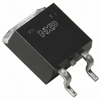
BUK116-50L,118 NXP Semiconductors, BUK116-50L,118 Datasheet - Page 2

BUK116-50L,118
Manufacturer Part Number
BUK116-50L,118
Description
TOPFET LOGIC LVL 50V D2PAK
Manufacturer
NXP Semiconductors
Series
TOPFET™r
Type
Low Sider
Datasheet
1.BUK116-50L118.pdf
(13 pages)
Specifications of BUK116-50L,118
Input Type
Non-Inverting
Number Of Outputs
1
On-state Resistance
22 mOhm
Current - Output / Channel
50A
Current - Peak Output
200A
Mounting Type
Surface Mount
Package / Case
D²Pak, TO-263 (4 leads + tab)
Lead Free Status / RoHS Status
Lead free / RoHS Compliant
Voltage - Supply
-
Operating Temperature
-
Other names
934044320118
BUK116-50L /T3
BUK116-50L /T3
BUK116-50L /T3
BUK116-50L /T3
Philips Semiconductors
LIMITING VALUES
Limiting values in accordance with the Absolute Maximum Rating System (IEC 134)
OVERLOAD PROTECTION LIMITING VALUES
With the protection supply
connected, TOPFET can protect
itself from two types of overload -
over temperature and short circuit
load.
ESD LIMITING VALUE
1 Prior to the onset of overvoltage clamping. For voltages above this value, safe operation is limited by the overvoltage clamping energy.
2 A higher T
3 The minimum supply voltage required for correct operation of the overload protection circuits.
4 The device is able to self-protect against a short circuit load providing the drain-source supply voltage does not exceed V
July 1996
Logic level TOPFET
SMD version of BUK106-50L/S
SYMBOL PARAMETER
V
V
V
V
I
I
I
P
T
T
T
SYMBOL PARAMETER
V
V
V
P
SYMBOL PARAMETER
V
D
D
DRM
stg
j
sold
DSS
IS
FS
PS
tot
PSP
DDP(T)
DDP(P)
DSM
C
For further information, refer to OVERLOAD PROTECTION CHARACTERISTICS.
j
is allowed as an overload condition but at the threshold T
Voltages
Continuous off-state drain source
voltage
Continuous input voltage
Continuous flag voltage
Continuous supply voltage
Currents
Continuous drain current
Continuous drain current
Repetitive peak on-state drain current T
Thermal
Total power dissipation
Storage temperature
Junction temperature
Lead temperature
Protection supply voltage
Over temperature protection
Protected drain source supply voltage V
Short circuit load protection
Protected drain source supply voltage
Instantaneous overload dissipation
Electrostatic discharge capacitor
voltage
1
2
3
An n-MOS transistor turns on
between the input and source to
quickly discharge the power
MOSFET gate capacitance.
4
CONDITIONS
V
T
T
T
continuous
during soldering
CONDITIONS
for valid protection
V
V
V
V
V
CONDITIONS
Human body model;
C = 250 pF; R = 1.5 k
-
-
-
-
IS
mb
mb
mb
mb
PS
IS
IS
PS
IS
IS
j(TO)
= 0 V
= 10 V; R
= 5 V; R
= 10 V; R
= 5 V; R
= 25 ˚C
= V
= V
2
25 ˚C
100 ˚C
25 ˚C
the over temperature trip operates to protect the switch.
PSN
PSN
; L
I
I
I
I
BUK116-50S
1 k
1 k
BUK116-50L
10 H
2 k
2 k
V
V
IS
IS
=
For internal overload protection to
remain latched while the control
circuit is high, external series input
resistance must be provided. Refer
to INPUT CHARACTERISTICS.
=
4.4
5.4
8
MIN.
MIN.
MIN.
-55
0
0
0
-
-
-
-
-
-
-
-
-
-
-
-
-
-
5
4
5
BUK116-50L/S
200 180
Product specification
50
31
8
MAX.
MAX.
MAX.
125
150
150
250
50
11
11
11
50
50
24
45
DDP(P)
4
2
-
-
-
45
28
5
maximum.
Rev 1.000
UNIT
UNIT
UNIT
kW
kV
˚C
˚C
˚C
W
V
V
V
V
V
A
A
A
V
V
V
V
V
V
V


