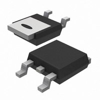
BUK139-50DL,118 NXP Semiconductors, BUK139-50DL,118 Datasheet - Page 2

BUK139-50DL,118
Manufacturer Part Number
BUK139-50DL,118
Description
MOSFET N-CH 50V 16A SOT428
Manufacturer
NXP Semiconductors
Series
TOPFET™r
Type
Low Sider
Datasheet
1.BUK139-50DL118.pdf
(6 pages)
Specifications of BUK139-50DL,118
Input Type
Non-Inverting
Number Of Outputs
1
On-state Resistance
36 mOhm
Current - Peak Output
24A
Mounting Type
Surface Mount
Package / Case
DPak, TO-252 (2 leads+tab), SC-63
Configuration
Single
Transistor Polarity
N-Channel
Resistance Drain-source Rds (on)
0.1 Ohms
Drain-source Breakdown Voltage
50 V
Continuous Drain Current
16 A
Power Dissipation
65 W
Maximum Operating Temperature
+ 150 C
Mounting Style
SMD/SMT
Minimum Operating Temperature
- 55 C
Lead Free Status / RoHS Status
Lead free / RoHS Compliant
Voltage - Supply
-
Operating Temperature
-
Current - Output / Channel
-
Lead Free Status / Rohs Status
Details
Other names
934056345118
BUK139-50DL /T3
BUK139-50DL /T3
BUK139-50DL /T3
BUK139-50DL /T3
Philips Semiconductors
LIMITING VALUES
Limiting values in accordance with the Absolute Maximum Rating System (IEC 134)
ESD LIMITING VALUE
OVERVOLTAGE CLAMPING LIMITING VALUES
At a drain source voltage above 50 V the power MOSFET is actively turned on to clamp overvoltage transients.
OVERLOAD PROTECTION LIMITING VALUE
With an adequate protection supply provided via the input pin, TOPFET can protect itself from two types of overload
- overtemperature and short circuit load.
THERMAL CHARACTERISTICS
1 Prior to the onset of overvoltage clamping. For voltages above this value, safe operation is limited by the overvoltage clamping energy.
2 A higher T
3 All control logic and protection functions are disabled during conduction of the source drain diode.
July 2001
Logic level TOPFET
D-PAK version of BUK118-50DL
SYMBOL PARAMETER
V
I
I
I
I
P
T
T
T
SYMBOL PARAMETER
V
SYMBOL PARAMETER
E
E
SYMBOL PARAMETER
V
SYMBOL PARAMETER
R
R
D
D
I
IRM
stg
j
sold
DS
D
C
DSM
DRM
DS
th j-mb
th j-a
j
is allowed as an overload condition but at the threshold T
Continuous drain source voltage
Continuous drain current
Continuous drain current
Continuous input current
Non-repetitive peak input current
Total power dissipation
Storage temperature
Continuous junction temperature
Case temperature
Electrostatic discharge capacitor
voltage
Inductive load turn-off
Non-repetitive clamping energy
Repetitive clamping energy
Drain source voltage
Thermal resistance
Junction to mounting base
Junction to ambient
3
1
2
CONDITIONS
minimum footprint FR4 PCB
-
CONDITIONS
V
V
T
normal operation
during soldering
CONDITIONS
Human body model;
C = 250 pF; R = 1.5 k
CONDITIONS
I
T
T
REQUIRED CONDITION
4 V
DM
-
-
t
mb
-
mb
mb
IS
IS
p
j(TO)
= 16 A; V
= 5 V; T
= 5 V; T
2
1 ms
25 ˚C
25 ˚C
95 ˚C; f = 250 Hz
V
the over temperature trip operates to protect the switch.
IS
5.5 V
mb
mb
DD
= 25 ˚C
125 ˚C
20 V
MIN.
MIN.
MIN.
MIN.
MIN.
-10
-55
-
-
-5
0
-
-
-
-
-
-
-
-
-
TYP.
1.75
71.4
BUK139-50DL
Product specification
limited
MAX.
MAX.
MAX.
MAX.
self -
175
150
260
200
50
16
10
65
32
35
5
2
MAX.
1.92
-
Rev 2.000
UNIT
UNIT
UNIT
UNIT
mA
mA
mJ
mJ
kV
UNIT
˚C
˚C
˚C
W
K/W
K/W
V
A
A
V


