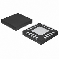
MAX4822ETP+ Maxim Integrated Products, MAX4822ETP+ Datasheet - Page 9

MAX4822ETP+
Manufacturer Part Number
MAX4822ETP+
Description
IC RELAY DRIVER 8CHAN 20-TQFN
Manufacturer
Maxim Integrated Products
Type
Relay/Lamp Driverr
Datasheet
1.MAX4823ETP.pdf
(19 pages)
Specifications of MAX4822ETP+
Input Type
Serial
Number Of Outputs
8
On-state Resistance
2.7 Ohm
Current - Output / Channel
70mA
Current - Peak Output
150mA
Voltage - Supply
2.3 V ~ 5.5 V
Operating Temperature
-40°C ~ 85°C
Mounting Type
Surface Mount
Package / Case
20-TQFN Exposed Pad
Lead Free Status / RoHS Status
Lead free / RoHS Compliant
Depending on the MAX4822/MAX4823 device, the serial
interface can be controlled by either 8- or 16-bit words
as depicted in Figures 1 and 2. The MAX4823 does not
support power-save mode, so the serial interface con-
sists of an 8-bit-only shift register for faster control.
The MAX4822 consists of a 16-bit shift register and par-
allel latch controlled by SCLK and CS. The input to the
shift register is a 16-bit word. In the MAX4822, the first
8 bits determine the register address and are followed
MAX4824
EP
13
14
15
17
18
19
20
—
+3.3V/+5V, 8-Channel Relay Drivers with Fast
Serial Interface (MAX4822/MAX4823)
PIN
MAX4825
14
15
17
18
19
20
13
EP
—
_______________________________________________________________________________________
Detailed Description
Recovery Time and Power-Save Mode
PSAVE
NAME
OUT4
OUT3
OUT2
OUT1
N.C.
V
SET
EP
CC
Power-Save Control. Connect a timing capacitor from PSAVE to ground. The capacitor
value determines power-save timing as explained under the Applications Information
section. PSAVE can also be driven externally to control power-save mode
asynchronously. When PSAVE is asserted high, the current through the coils is reduced
to 60% of the initial nominal current value. To disable power-save mode in all channels,
drive PSAVE low for at least 3ms after last output setting.
Open-Drain Output 4. Connect OUT4 to the low side of a relay coil. This output is pulled
to PGND when activated, but otherwise is high impedance.
Open-Drain Output 3. Connect OUT3 to the low side of a relay coil. This output is pulled
to PGND when activated, but otherwise is high impedance.
Open-Drain Output 2. Connect OUT2 to the low side of a relay coil. This output is pulled
to PGND when activated, but otherwise is high impedance.
Open-Drain Output 1. Connect OUT1 to the low side of a relay coil. This output is pulled
to PGND when activated, but otherwise is high impedance.
Input Supply Voltage. Bypass V
Set Input. Drive SET low to set all latches and registers high (all outputs are low
impedance). SET overrides all parallel and serial control inputs. RESET overrides SET
under all conditions.
No Connection. Not internally connected.
Exposed Pad. Connect exposed paddle to ground.
MAX4824/MAX4825 Pin Description (continued)
by 8 bits of data as depicted in Figure 1. Bit A7 corre-
sponds to the MSB of the 8-bit register address in
Figure 1, while bit D7 corresponds to the MSB of the 8
bits of data in the same Figure 1.
The MAX4823 consists of an 8-bit shift register and par-
allel latch controlled by SCLK and CS. The input to the
shift register is an 8-bit word. Each data bit controls
one of the eight outputs, with the most significant bit
(D7) corresponding to OUT8, and the least significant
bit (D0) corresponding to OUT1 (see Figure 2).
CC
to GND with a 0.1µF capacitor.
FUNCTION
9


