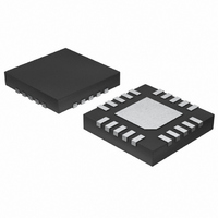
MAX4822ETP+ Maxim Integrated Products, MAX4822ETP+ Datasheet - Page 13

MAX4822ETP+
Manufacturer Part Number
MAX4822ETP+
Description
IC RELAY DRIVER 8CHAN 20-TQFN
Manufacturer
Maxim Integrated Products
Type
Relay/Lamp Driverr
Datasheet
1.MAX4823ETP.pdf
(19 pages)
Specifications of MAX4822ETP+
Input Type
Serial
Number Of Outputs
8
On-state Resistance
2.7 Ohm
Current - Output / Channel
70mA
Current - Peak Output
150mA
Voltage - Supply
2.3 V ~ 5.5 V
Operating Temperature
-40°C ~ 85°C
Mounting Type
Surface Mount
Package / Case
20-TQFN Exposed Pad
Lead Free Status / RoHS Status
Lead free / RoHS Compliant
connected to PSAVE. The value t
lowing formula:
where C is in µF and t
For example, if the desired t
required capacitor value is 20 / 32 = 0.625µF.
The current through the relay is controlled by setting
the voltage at OUT_ to a percentage of the V
as specified under the Electrical Characteristics and in
the register description. The current through the relay
(I
addition to the relay resistance R
lowing relation:
The power-save, current-setting I
fraction
loop depending on the following relation:
Therefore:
This relation shows how the fraction of reduction in the
current depends on the switch on-resistance, as well as
from the accuracy of the voltage setting ( ). The higher
the R
This is particularly true at low voltage when the relay
resistance is low (less than 40 ) and the switch can
account for up to 10% of the total resistance. In addi-
tion, when the supply-voltage setting ( ) is low (10% or
20%) and the supply voltage (V
drop across the switch (I
exceed, or may be very close to, the desired voltage-
setting value.
In a normal configuration using the power-save feature,
several MAX4822s can be daisy chained as shown in
Figure 9. For each MAX4822, the power-save timing
t
relay is actuated) is controlled by the capacitor con-
nected to PSAVE.
An alternative configuration that eliminates the PSAVE
capacitors uses a common PSAVE control line driven by
an open-drain n-channel MOSFET (Figure 10). In this con-
figuration, the PSAVE inputs are connected together to
asynchronously control the power-save timing for all the
MAX4822s in the chain. The µC/µP drives the n-channel
MOSFET low for the duration of a write cycle to the SPI
chain, plus some delay time to allow the relays to close.
PD
OUT
(time it takes to reduce the relay current once the
ON
) depends on the switch on-resistance, R
+3.3V/+5V, 8-Channel Relay Drivers with Fast
Daisy Chaining and Power-Save Mode
with respect to R
of the supply voltage V
I
PS
/ I
I
I
PS
OUT
OUT
______________________________________________________________________________________
= V
= V
= (1- ) x (1 + R
t
PS
CC
PS
CC
Recovery Time and Power-Save Mode
is in ms.
- ( x V
= 32 x C
Power-Save Mode Accuracy
R,
/ (R
OUT
the higher the inaccuracy.
ON
PS
CC
CC
R
x R
PS
+ R
CC
according to the fol-
PS
) / R
) is low, the voltage
is 20ms, then the
ON
is given by the fol-
ON
R
that is set by the
depends on the
)
R
/ R
) may already
R
)
CC
supply
ON,
in
(This time is typically specified in the relay data sheet.)
Once this delay time has elapsed, the n-channel MOSFET
is turned off, allowing the MAX4822’s internal 35µA pullup
current to raise PSAVE to a logic-high level, activating the
power-save mode in all active outputs.
In the daisy-chain configuration of Figure 10, the n-channel
MOSFET drives PSAVE low. When the n-channel
MOSFET is turned off, PSAVE is pulled high by an internal
35µA pullup in each MAX4822, and the power-save mode
is enabled. Because of the paralleled PSAVE pullup
currents, the required size of the n-channel MOSFET
depends upon the number of MAX4822 devices in the
chain. Determine the size of the n-channel MOSFET by the
following relation:
Figure 6. 3-Wire Serial-Interface Operation for the MAX4823
Figure 7. Parallel-Interface Timing Diagram
SCLK
DIN
CS
V
LVL
OUT
CS
A_
D7
t
D6
AS
R
ON
D5
< 1428 / N
D4
D3
MOSFET Selection
D2
t
LS
D1
t
t
t
t
OFF
ON
AH
LH
D0
,
13


