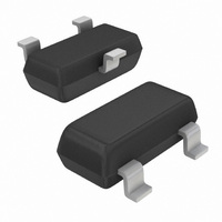
NUD3105LT1G ON Semiconductor, NUD3105LT1G Datasheet - Page 3

NUD3105LT1G
Manufacturer Part Number
NUD3105LT1G
Description
IC INDUCTIVE LOAD DRVR 6V SOT23
Manufacturer
ON Semiconductor
Type
Low Sider
Datasheet
1.NUD3105LT1G.pdf
(8 pages)
Specifications of NUD3105LT1G
Input Type
Non-Inverting
Number Of Outputs
1
On-state Resistance
900 mOhm
Current - Output / Channel
400mA
Current - Peak Output
500mA
Operating Temperature
-40°C ~ 85°C
Mounting Type
Surface Mount
Package / Case
SOT-23-3, TO-236-3, Micro3™, SSD3, SST3
Configuration
Single
Transistor Polarity
N-Channel
Resistance Drain-source Rds (on)
0.9 Ohm @ 5 V
Drain-source Breakdown Voltage
6 V
Gate-source Breakdown Voltage
6 V
Continuous Drain Current
0.5 A
Power Dissipation
225 mW
Maximum Operating Temperature
+ 85 C
Mounting Style
SMD/SMT
Minimum Operating Temperature
- 40 C
Supply Voltage Max
6V
No. Of Outputs
1
Output Voltage
6V
Output Current
400mA
Driver Case Style
SOT-23
Device Type
Relay
Termination Type
SMD
No. Of Pins
3
Rohs Compliant
Yes
Filter Terminals
SMD
Leaded Process Compatible
Yes
Lead Free Status / RoHS Status
Lead free / RoHS Compliant
Voltage - Supply
-
Lead Free Status / Rohs Status
Lead free / RoHS Compliant
Other names
NUD3105LT1GOS
NUD3105LT1GOS
NUD3105LT1GOSTR
NUD3105LT1GOS
NUD3105LT1GOSTR
Available stocks
Company
Part Number
Manufacturer
Quantity
Price
Company:
Part Number:
NUD3105LT1G
Manufacturer:
ON
Quantity:
1 290
Part Number:
NUD3105LT1G
Manufacturer:
ON/安森美
Quantity:
20 000
ELECTRICAL CHARACTERISTICS (T
DYNAMIC CHARACTERISTICS
SWITCHING CHARACTERISTICS
Input Capacitance
Output Capacitance
Transfer Capacitance
Propagation Delay Times:
Transition Times:
(V
(V
(V
High to Low Propagation Delay; Figure 1 (5.0 V)
Low to High Propagation Delay; Figure 1 (5.0 V)
High to Low Propagation Delay; Figure 1 (3.0 V)
Low to High Propagation Delay; Figure 1 (3.0 V)
Fall Time; Figure 1 (5.0 V)
Rise Time; Figure 1 (5.0 V)
Fall Time; Figure 1 (3.0 V)
Rise Time; Figure 1 (3.0 V)
DS
DS
DS
= 5.0 V,V
= 5.0 V, V
= 5.0 V, V
GS
GS
GS
= 0 V, f = 10 kHz)
= 0 V, f = 10 kHz)
= 0 V, f = 10 kHz)
V
V
out
in
50%
Characteristic
Characteristic
90%
t
PHL
J
= 25°C unless otherwise noted)
Figure 1. Switching Waveforms
t
f
50%
http://onsemi.com
10%
3
t
PLH
Symbol
Symbol
C
t
t
t
t
C
C
PHL
PLH
PHL
PLH
oss
t
tr
t
t
t
rss
iss
r
f
f
r
Min
Min
−
−
−
−
−
−
−
−
−
−
−
V
0 V
V
V
IH
OH
OL
Typ
Typ
8.0
25
37
25
80
44
44
23
32
53
30
Max
Max
−
−
−
−
−
−
−
−
−
−
−
Units
Unit
pF
pF
pF
nS
nS


