NUD3105LT1G ON Semiconductor, NUD3105LT1G Datasheet - Page 2
NUD3105LT1G
Manufacturer Part Number
NUD3105LT1G
Description
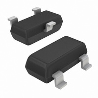
IC INDUCTIVE LOAD DRVR 6V SOT23
Manufacturer
ON Semiconductor
Type
Low Sider
Datasheet
1.NUD3105LT1G.pdf
(8 pages)
Specifications of NUD3105LT1G
Input Type
Non-Inverting
Number Of Outputs
1
On-state Resistance
900 mOhm
Current - Output / Channel
400mA
Current - Peak Output
500mA
Operating Temperature
-40°C ~ 85°C
Mounting Type
Surface Mount
Package / Case
SOT-23-3, TO-236-3, Micro3™, SSD3, SST3
Configuration
Single
Transistor Polarity
N-Channel
Resistance Drain-source Rds (on)
0.9 Ohm @ 5 V
Drain-source Breakdown Voltage
6 V
Gate-source Breakdown Voltage
6 V
Continuous Drain Current
0.5 A
Power Dissipation
225 mW
Maximum Operating Temperature
+ 85 C
Mounting Style
SMD/SMT
Minimum Operating Temperature
- 40 C
Supply Voltage Max
6V
No. Of Outputs
1
Output Voltage
6V
Output Current
400mA
Driver Case Style
SOT-23
Device Type
Relay
Termination Type
SMD
No. Of Pins
3
Rohs Compliant
Yes
Filter Terminals
SMD
Leaded Process Compatible
Yes
Lead Free Status / RoHS Status
Lead free / RoHS Compliant
Voltage - Supply
-
Lead Free Status / Rohs Status
Lead free / RoHS Compliant
Other names
NUD3105LT1GOS
NUD3105LT1GOS
NUD3105LT1GOSTR
NUD3105LT1GOS
NUD3105LT1GOSTR
Available stocks
Company
Part Number
Manufacturer
Quantity
Price
Company:

Part Number:
NUD3105LT1G
Manufacturer:
ON
Quantity:
1 290
Part Number:
NUD3105LT1G
Manufacturer:
ON/安森美
Quantity:
20 000


Stresses exceeding Maximum Ratings may damage the device. Maximum Ratings are stress ratings only. Functional operation above the
Recommended Operating Conditions is not implied. Extended exposure to stresses above the Recommended Operating Conditions may affect
device reliability.
1. This device contains ESD protection and exceeds the following tests:
2. Refer to the section covering Avalanche and Energy.
MAXIMUM RATINGS (T
ELECTRICAL CHARACTERISTICS (T
OFF CHARACTERISTICS
ON CHARACTERISTICS
Drain to Source Voltage − Continuous
Gate to Source Voltage – Continuous
Drain Current – Continuous
Single Pulse Drain−to−Source Avalanche Energy (
Repetitive Pulse Zener Energy Limit (DC v 0.01%) (f = 100 Hz, DC = 0.5)
Junction Temperature
Operating Ambient Temperature
Storage Temperature Range
Total Power Dissipation (Note 1)
Derating Above 25°C
Thermal Resistance, Junction−to−Ambient
Drain to Source Sustaining Voltage (Internally Clamped), (I D = 10 mA)
I
Drain to Source Leakage Current
Gate Body Leakage Current
Gate Threshold Voltage
Drain to Source On−Resistance
Output Continuous Current
Forward Transconductance
g
= 1.0 mA
(V
(V
(V
(V
(V
(V
(I
(I
(I
(I
(I
(V
(V
(V
D
D
D
D
D
Human Body Model 2000 V per MIL_STD−883, Method 3015.
Machine Model Method 200 V.
DS
DS
GS
GS
GS
GS
DS
DS
OUT
= 250 mA, V
= 500 mA, V
= 500 mA, V
= 500 mA, V
= 500 mA, V
= 5.5 V , V
= 5.5 V, V
= 0.25 V, V
= 0.25 V, V
= 3.0 V, V
= 5.0 V, V
= V
= V
= 5.0 V, I
DS
DS
, I
, I
D
D
GS
DS
DS
= 1.0 mA)
= 1.0 mA, T
OUT
GS
GS
GS
GS
GS
GS
GS
GS
= 0 V, T
= 0 V)
= 0 V)
= 3.0 V)
= 3.0 V)
= 5.0 V)
= 3.0 V, T
= 5.0 V, T
= 0 V, T
= 3.0 V)
= 3.0 V, T
= 0.25 A)
J
= 25°C unless otherwise specified)
J
J
J
= 85°C )
= 25°C)
= 85°C)
J
J
J
=85°C)
=85°C)
Characteristic
= 85°C)
Rating
J
= 25°C unless otherwise noted)
T
Jinitial =
http://onsemi.com
25°C) (Note 2)
2
Symbol
Symbol
V
R
V
B
I
V
DS(on)
BRDSS
R
I
V
E
I
DS(on)
GS(th)
T
VGSO
g
DSS
GSS
P
T
T
DSS
E
I
qJA
GS
zpk
stg
FS
D
A
D
J
z
Min
300
200
350
6.0
5.0
0.8
0.8
−
−
−
−
−
−
−
−
−
−65 to +150
−40 to 85
Value
500
150
225
556
Typ
400
570
6.0
6.0
4.5
1.8
8.0
1.2
50
−
−
−
−
−
−
−
−
−
−
−
−
Max
9.0
8.0
1.4
1.4
1.2
1.3
0.9
1.3
0.9
15
15
19
50
−
−
−
mW/°C
mmhos
°C/W
Unit
Unit
mW
V
V
mA
mA
mJ
mJ
°C
°C
°C
mA
mA
W
V
V
V
dc
dc
Related parts for NUD3105LT1G
Image
Part Number
Description
Manufacturer
Datasheet
Request
R

Part Number:
Description:
ON Semiconductor [VOLTAGE REGULATOR]
Manufacturer:
ON Semiconductor
Datasheet:
Part Number:
Description:
357-036-542-201 CARDEDGE 36POS DL .156 BLK LOPRO
Manufacturer:
ON Semiconductor
Datasheet:
Part Number:
Description:
357-036-542-201 CARDEDGE 36POS DL .156 BLK LOPRO
Manufacturer:
ON Semiconductor
Datasheet:
Part Number:
Description:
357-036-542-201 CARDEDGE 36POS DL .156 BLK LOPRO
Manufacturer:
ON Semiconductor
Datasheet:
Part Number:
Description:
357-036-542-201 CARDEDGE 36POS DL .156 BLK LOPRO
Manufacturer:
ON Semiconductor
Datasheet:
Part Number:
Description:
357-036-542-201 CARDEDGE 36POS DL .156 BLK LOPRO
Manufacturer:
ON Semiconductor
Datasheet:
Part Number:
Description:
357-036-542-201 CARDEDGE 36POS DL .156 BLK LOPRO
Manufacturer:
ON Semiconductor
Datasheet:
Part Number:
Description:
357-036-542-201 CARDEDGE 36POS DL .156 BLK LOPRO
Manufacturer:
ON Semiconductor
Datasheet:
Part Number:
Description:
357-036-542-201 CARDEDGE 36POS DL .156 BLK LOPRO
Manufacturer:
ON Semiconductor
Datasheet:
Part Number:
Description:
357-036-542-201 CARDEDGE 36POS DL .156 BLK LOPRO
Manufacturer:
ON Semiconductor
Datasheet:
Part Number:
Description:
357-036-542-201 CARDEDGE 36POS DL .156 BLK LOPRO
Manufacturer:
ON Semiconductor
Datasheet:
Part Number:
Description:
Manufacturer:
ON Semiconductor
Datasheet:
Part Number:
Description:
Manufacturer:
ON Semiconductor
Datasheet: