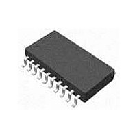
MC33186VW1R2 Freescale Semiconductor, MC33186VW1R2 Datasheet - Page 4

MC33186VW1R2
Manufacturer Part Number
MC33186VW1R2
Description
IC DRIVER H-BRIDGE 20-HSOP
Manufacturer
Freescale Semiconductor
Type
H Bridger
Datasheet
1.MC33186VW1.pdf
(21 pages)
Specifications of MC33186VW1R2
Input Type
Non-Inverting
Number Of Outputs
2
On-state Resistance
150 mOhm
Current - Output / Channel
5A
Current - Peak Output
6.5A
Voltage - Supply
5 V ~ 28 V
Operating Temperature
-40°C ~ 125°C
Mounting Type
Surface Mount
Package / Case
20-HSOP
Supply Voltage (min)
5 V
Maximum Operating Temperature
+ 125 C
Mounting Style
SMD/SMT
Bridge Type
H Bridge
Minimum Operating Temperature
- 40 C
Number Of Drivers
4
Lead Free Status / RoHS Status
Contains lead / RoHS non-compliant
Table 1. 33186 Pin Description(continued)
4
33186
PIN CONNECTIONS
4, 5, 16
Pin
17
Name
VBAT
CP
The Pins 4 and 5 are internally connected. These Pins supply the left high side and the analog/logic
part of the device.
The Pin 16 supplies the right high side and the charge pump.
The Pins 4, 5 and 16 should be connected together on the printed circuit board with connections as
short as possible.
Supervision and protection functions
a) Supply voltage supervision
The supply voltage is supervised. If it is below its specific threshold, the power stages are switched
in tristate and the status flag is switched low.
If the supply voltage is over the specific threshold again, the power stage switches independently
into normal operation, according to the input Pins and the status flag is reset.
b) Thermal supervision
In case of overtemperature, the power stages are switched in tristate independent of the inputs
signals and the status flag is switched low.
If the level changes from high to low on DI1 (IN1) or low to high on DI2 (IN2), the output stage
switches on again if the temperature is below the specified limit.The status-flag is reset to high level
(Pin names in brackets refer to coding Pin = VCC).
c) Supervision of overcurrent on high sides and low sides
In case of over-current detection, the power stages are switched in tristate independent of the inputs
signals and the status flag is set.
If the level changes from high to low on DI1 (IN1) or low to high on DI2 (IN2) the output stage
switches on again and the status flag is reset to high level (Pin names in brackets refer to coding Pin
= VCC).
The output stage switches into the mode defined by the inputs Pins provided, and/if the temperature
is below the specified limits.
d) Current limiting on low sides
The maximum current which can flow under normal operating conditions is limited to Imax = 6,5 A
+/- 20%. When the maximum current value is reached, the output stages are switched tristate for a
fixed time. According to the time constant the current decreases until the next switch on occurs. See
page 8 for schematics.
Charge Pump output Pin
A filtering capacitor (up to 33 nF) can be connected between Pin 17 and Gnd. Device can operate
without external capacitor, although Pin 17 decoupling capacitor help in noise reduction and allows
the device to perform a maximum speed, timing and PWM frequency.
Description
Analog Integrated Circuit Device Data
Freescale Semiconductor


