VNQ5050KTR-E STMicroelectronics, VNQ5050KTR-E Datasheet - Page 9
VNQ5050KTR-E
Manufacturer Part Number
VNQ5050KTR-E
Description
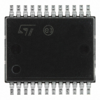
IC DRIVER HISIDE QUAD POWERSSO24
Manufacturer
STMicroelectronics
Type
High Sider
Datasheet
1.VNQ5050KTR-E.pdf
(31 pages)
Specifications of VNQ5050KTR-E
Input Type
Non-Inverting
Number Of Outputs
4
On-state Resistance
50 mOhm
Current - Peak Output
19A
Voltage - Supply
4.5 V ~ 36 V
Operating Temperature
-40°C ~ 150°C
Mounting Type
Surface Mount
Package / Case
PowerSSO-24
Number Of Drivers
4
Driver Configuration
Non-Inverting
Driver Type
High Side
Input Logic Level
CMOS
Operating Supply Voltage (max)
36V
Peak Output Current
12A
Operating Supply Voltage (min)
4.5V
Operating Supply Voltage (typ)
13V
Turn Off Delay Time
40us
Turn On Delay Time (max)
15us
Operating Temp Range
-40C to 150C
Operating Temperature Classification
Automotive
Mounting
Surface Mount
Pin Count
24
Package Type
PowerSSO
Supply Voltage (min)
4.5 V
Supply Current
14 mA
Maximum Operating Temperature
+ 150 C
Mounting Style
SMD/SMT
Maximum Turn-off Delay Time
40000 ns
Maximum Turn-on Delay Time
15000 ns
Minimum Operating Temperature
- 40 C
Lead Free Status / RoHS Status
Lead free / RoHS Compliant
Current - Output / Channel
-
Lead Free Status / Rohs Status
Compliant
Available stocks
Company
Part Number
Manufacturer
Quantity
Price
Company:

Part Number:
VNQ5050KTR-E
Manufacturer:
st
Quantity:
5 000
Company:
Part Number:
VNQ5050KTR-E
Manufacturer:
STM
Quantity:
294
Part Number:
VNQ5050KTR-E
Manufacturer:
ST
Quantity:
20 000


VNQ5050K-E
2.3
Electrical characteristics
Values specified in this section are for 8 V<V
stated.
Table 6.
1. For each channel.
2. PowerMOS leakage included
Table 7.
V
dV
dV
Symbol
V
I
I
USDhyst
V
Symbol
L(off1)
L(off2)
V
R
OUT
OUT
clamp
W
V
USD
t
t
W
I
CC
ON
d(on)
d(off)
S
F
OFF
ON
/dt
/dt
(on)
(off)
Operating supply voltage
Undervoltage shutdown
Undervoltage shutdown
hysteresis
On-state resistance
Clamp Voltage
Supply current
Off-state output current
Off-state output current
Output - V
voltage
Turn-on delay time
Turn-off delay time
Turn-on voltage slope
Turn-off voltage slope
Switching energy
losses during t
Switching energy
losses during t
Power section
Switching (V
Parameter
(1)
Parameter
CC
diode
won
woff
CC
(1)
=13V; T
Doc ID 10864 Rev 6
(1)
(1)
R
(see
R
(see
R
(See
R
(See
R
(see
R
(see
I
I
I
I
Off-state; V
V
On-state; V
I
V
V
T
V
-I
OUT
OUT
OUT
S
OUT
j
OUT
IN
IN
IN
IN
L
L
L
L
L
L
=20 mA
=125°C
=6.5Ω
=6.5Ω
=6.5Ω
=6.5Ω
=6.5Ω
=6.5Ω
j
=V
=V
=V
=0V; V
=25°C)
=2A; T
=2A; T
=2A; V
=0A
Figure
Figure
Figure
Figure
=2A; T
Figure
Figure
OUT
OUT
OUT
Test conditions
Test conditions
=0V; T
=0V; V
=0V; V
OUT
j
j
CC
CC
CC
IN
=25°C
=150°C
j
6)
6)
6)
6)
=150°C
16)
18)
=5V; V
= 4V
=5V; T
=13V;
<36 V, -40 °C< T
j
CC
CC
=25°C
=13V; T
=13V;
CC
j
=25°C
=13V;
j
=25°C
j
Min.
<150 °C, unless otherwise
Electrical specifications
-
-
-
-
-
-
Min. Typ.
4.5
-75
41
0
0
Typ.
0.19
0.27
0.01
15
40
2
3.5
0.5
13
46
8
(2)
Max.
Max.
100
5
4.5
0.7
36
50
65
52
14
-
-
-
-
-
-
3
5
0
(2)
Unit
V/μs
V/μs
Unit
mΩ
mΩ
mΩ
mJ
mJ
mA
μs
μs
μA
μA
μA
μA
V
V
V
V
V
9/31
Related parts for VNQ5050KTR-E
Image
Part Number
Description
Manufacturer
Datasheet
Request
R

Part Number:
Description:
IC DRIVER HISIDE QUAD POWERSSO24
Manufacturer:
STMicroelectronics
Datasheet:

Part Number:
Description:
STMicroelectronics [RIPPLE-CARRY BINARY COUNTER/DIVIDERS]
Manufacturer:
STMicroelectronics
Datasheet:
Part Number:
Description:
STMicroelectronics [LIQUID-CRYSTAL DISPLAY DRIVERS]
Manufacturer:
STMicroelectronics
Datasheet:

Part Number:
Description:
BOARD EVAL FOR MEMS SENSORS
Manufacturer:
STMicroelectronics
Datasheet:
Part Number:
Description:
NPN TRANSISTOR POWER MODULE
Manufacturer:
STMicroelectronics
Datasheet:
Part Number:
Description:
TURBOSWITCH ULTRA-FAST HIGH VOLTAGE DIODE
Manufacturer:
STMicroelectronics
Datasheet:
Part Number:
Description:
Manufacturer:
STMicroelectronics
Datasheet:
Part Number:
Description:
DIODE / SCR MODULE
Manufacturer:
STMicroelectronics
Datasheet:
Part Number:
Description:
DIODE / SCR MODULE
Manufacturer:
STMicroelectronics
Datasheet:
Part Number:
Description:
Search -----> STE16N100
Manufacturer:
STMicroelectronics
Datasheet:
Part Number:
Description:
Search ---> STE53NA50
Manufacturer:
STMicroelectronics
Datasheet: