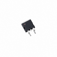
VNB35NV04TR-E STMicroelectronics, VNB35NV04TR-E Datasheet

VNB35NV04TR-E
Specifications of VNB35NV04TR-E
Available stocks
Related parts for VNB35NV04TR-E
VNB35NV04TR-E Summary of contents
Page 1
... ESD PROTECTION n DIRECT ACCESS TO THE GATE OF THE POWER MOSFET (ANALOG DRIVING) n COMPATIBLE WITH STANDARD POWER MOSFET DESCRIPTION The VNB35NV04, VNP35NV04, VNV35NV04, VNW35NV04 are monolithic devices designed in STMicroelectronics VIPower M0-3 Technology, BLOCK DIAGRAM INPUT 1 March 2004 VNB35NV04 / VNP35NV04 / VNV35NV04 / VNW35NV04 V lim clamp ...
Page 2
VNB35NV04 / VNP35NV04 / VNV35NV04 / VNW35NV04 ABSOLUTE MAXIMUM RATING Symbol Parameter V Drain-source Voltage ( Input Voltage IN I Input Current IN R Minimum Input Series Impedance IN MIN I Drain Current D I Reverse DC Output ...
Page 3
THERMAL DATA Symbol Parameter R Thermal Resistance Junction-case}}} thj-case R Thermal Resistance Junction-ambient MAX thj-amb When mounted on a standard single-sided FR4 board with 50mm (*) ELECTRICAL CHARACTERISTICS (-40°C < T OFF Symbol Parameter Drain-source Clamp V CLAMP Voltage Drain-source ...
Page 4
VNB35NV04 / VNP35NV04 / VNV35NV04 / VNW35NV04 ELECTRICAL CHARACTERISTICS (continued) (T DYNAMIC Symbol Parameter Forward g (*) fs Transconductance C Output Capacitance OSS SWITCHING Symbol Parameter t Turn-on Delay Time d(on) t Rise Time r t Turn-off Delay Time d(off) ...
Page 5
PROTECTION FEATURES During normal operation, the INPUT pin is electrically connected to the gate of the internal power MOSFET through a low impedance path. The device then behaves like a standard power MOSFET and can be used as a switch ...
Page 6
VNB35NV04 / VNP35NV04 / VNV35NV04 / VNW35NV04 Fig.1: Switching Time Test Circuit for Resistive Load d(on) V gen Fig.2: Test Circuit for Diode Recovery Times I OMNIFET 25 6/ gen V gen ...
Page 7
Fig. 3: Unclamped Inductive Load Test Circuits R GEN Fig. 5: Input Charge Test Circuit GEN V IN Fig. 7:Thermal Impedance for TO-247 VNB35NV04 / VNP35NV04 / VNV35NV04 / VNW35NV04 Fig. 4: Unclamped Inductive Waveforms Fig ...
Page 8
VNB35NV04 / VNP35NV04 / VNV35NV04 / VNW35NV04 Source-Drain Diode Forward Characteristics Vsd (mV) 950 900 Vin=0V 850 800 750 700 650 (A) PowerSO-10 Static Drain-Source On resistance Vs. Input Voltage Rds(on) (mOhm) 27.5 25 ...
Page 9
Transconductance Gfs ( Vds=13V (A) Output Characteristics Id ( Vin=4V 45 Vin=4.5V Vin=3.5V 40 Vin= ...
Page 10
VNB35NV04 / VNP35NV04 / VNV35NV04 / VNW35NV04 Input Voltage Vs. Input Charge Vin ( Vds=12V Id=15A 100 Qg (nC) Turn Off Drain-Source Voltage Slope dV/dt (V/us) 160 ...
Page 11
Current Limit Vs. Junction Temperature Ilim (A) 100 90 Vin=6V Vds=13V -50 - (ºC) Derating Curve VNB35NV04 / VNP35NV04 / VNV35NV04 / VNW35NV04 Step Response Current ...
Page 12
VNB35NV04 / VNP35NV04 / VNV35NV04 / VNW35NV04 DIM L20 L30 P Q Package Weight 12/19 TO-220 MECHANICAL DATA mm. MIN. TYP 4.40 0.61 1.15 0.49 15.25 10 ...
Page 13
TO-247 MECHANICAL DATA DIM. MIN. A 4.7 D 2 15.3 L 19 Dia. 3. VNB35NV04 / VNP35NV04 / VNV35NV04 / VNW35NV04 mm. ...
Page 14
VNB35NV04 / VNP35NV04 / VNV35NV04 / VNW35NV04 PowerSO-10™ MECHANICAL DATA DIM. MIN. A 3.35 A (*) 3.4 A1 0.00 B 0.40 B (*) 0.37 C 0.35 C (*) 0.23 D 9.40 D1 7.40 E 9.30 E2 7.20 E2 (*) 7.30 ...
Page 15
VNB35NV04 / VNP35NV04 / VNV35NV04 / VNW35NV04 2 D PAK MECHANICAL DATA DIM. MIN. A 4.4 A1 2.49 A2 0.03 B 0.7 B2 1.14 C 0.45 C2 1. 1.27 ...
Page 16
VNB35NV04 / VNP35NV04 / VNV35NV04 / VNW35NV04 TO-220 TUBE SHIPMENT (no suffix 16/19 Base Q.ty Bulk Q.ty Tube length (± 0. (± 0.1) All dimensions are in mm 1000 532 5.5 31.4 0.75 ...
Page 17
SUGGESTED PAD LAYOUT PowerSO-10™ 14.6 - 14 TAPE AND REEL SHIPMENT (suffix “13TR”) TAPE DIMENSIONS According to Electronic Industries Association (EIA) Standard 481 rev. A, ...
Page 18
VNB35NV04 / VNP35NV04 / VNV35NV04 / VNW35NV04 2 D PAK FOOTPRINT 16.90 12.20 3.50 9.75 All dimensions are in millimeters TAPE AND REEL SHIPMENT (suffix “13TR”) TAPE DIMENSIONS According to Electronic Industries Association (EIA) Standard 481 rev. A, Feb 1986 ...
Page 19
... STMicroelectronics. Specifications mentioned in this publication are subject to change without notice. This publication supersedes and replaces all information previously supplied. STMicroelectronics products are not authorized for use as critical components in life support devices or systems without express written approval of STMicroelectronics. 2004 STMicroelectronics - Printed in ITALY- All Rights Reserved. ...


