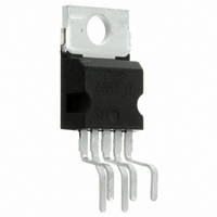
VN920-E STMicroelectronics, VN920-E Datasheet - Page 16

VN920-E
Manufacturer Part Number
VN920-E
Description
IC DRIVER HIGH SIDE PENTAWATT-5
Manufacturer
STMicroelectronics
Type
High Sider
Datasheet
1.VN920B5TR-E.pdf
(23 pages)
Specifications of VN920-E
Input Type
Non-Inverting
Number Of Outputs
1
On-state Resistance
16 mOhm
Current - Output / Channel
45A
Voltage - Supply
5.5 V ~ 36 V
Operating Temperature
-40°C ~ 150°C
Mounting Type
Through Hole
Package / Case
Pentawatt-5 (Vertical, Bent and Staggered Leads)
Switch Type
High Side
Power Switch Family
VN920
Power Switch On Resistance
16mOhm
Output Current
30A
Mounting
Through Hole
Supply Current
5mA
Package Type
Pentawatt
Operating Temperature (min)
-40C
Operating Temperature (max)
150C
Operating Temperature Classification
Automotive
Pin Count
5 +Tab
Power Dissipation
96.1W
Supply Voltage (min)
5.5 V
Maximum Power Dissipation
96100 mW
Maximum Operating Temperature
+ 150 C
Mounting Style
Through Hole
Minimum Operating Temperature
- 40 C
Device Type
High Side
Module Configuration
High Side
Peak Output Current
45A
Output Resistance
0.016ohm
Input Delay
50µs
Output Delay
50µs
Supply Voltage Range
5.5V To 36V
Rohs Compliant
Yes
Lead Free Status / RoHS Status
Lead free / RoHS Compliant
Current - Peak Output
-
Lead Free Status / Rohs Status
Compliant
Application information
3
3.1
3.1.1
16/23
Application information
Figure 19. Application schematic
GND protection network against reverse battery
Solution 1: resistor in the ground line (R
This can be used with any type of load.
The following is an indication on how to dimension the R
1.
2.
where - I
maximum rating section of the device datasheet.
Power Dissipation in R
P
This resistor can be shared amongst several different HSDs. Please note that the value of
this resistor should be calculated with formula (1) where I
maximum on-state currents of the different devices.
Please note that if the microprocessor ground is not shared by the device ground then the
R
values. This shift will vary depending on how many devices are ON in the case of several
high-side drivers sharing the same R
If the calculated power dissipation leads to a large resistor or several devices have to share
the same resistor then ST suggests to utilize Solution 2 (see below).
D
GND
= (- V
R
R
+5V
μC
will produce a shift (I
GND
GND
CC
GND
≤ 600mV / (I
≥ (- V
)
2
/ R
is the DC reverse ground pin current and can be found in the absolute
GND
R
R
CC
prot
prot
R
SENSE
) / (- I
GND
S(on)max
GND
S(on)max
(when V
)
INPUT
CURRENT SENSE
Doc ID 10894 Rev 3
).
* R
CC
GND
GND
< 0: during reverse battery situations) is:
.
) in the input thresholds and the status output
V
GND
R
GND
GND
GND
GND
S(on)max
only)
V
CC
resistor.
D
GND
becomes the sum of the
OUTPUT
VN920-E
D
ld


