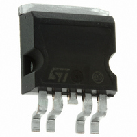
VN920B5TR-E STMicroelectronics, VN920B5TR-E Datasheet - Page 8

VN920B5TR-E
Manufacturer Part Number
VN920B5TR-E
Description
IC DRIVER HIGH SIDE P2PAK
Manufacturer
STMicroelectronics
Type
High Sider
Specifications of VN920B5TR-E
Input Type
Non-Inverting
Number Of Outputs
1
On-state Resistance
16 mOhm
Current - Output / Channel
45A
Voltage - Supply
5.5 V ~ 36 V
Operating Temperature
-40°C ~ 150°C
Mounting Type
Surface Mount
Package / Case
P²PAK (4 leads + Tab)
Supply Voltage (min)
5.5 V
Supply Current
5 mA
Maximum Power Dissipation
96100 mW
Maximum Operating Temperature
+ 150 C
Mounting Style
SMD/SMT
Minimum Operating Temperature
- 40 C
Switch Type
High Side
Power Switch Family
VN920
Power Switch On Resistance
16mOhm
Output Current
30A
Mounting
Surface Mount
Package Type
P2PAK
Operating Temperature (min)
-40C
Operating Temperature (max)
150C
Operating Temperature Classification
Automotive
Pin Count
4 +Tab
Power Dissipation
96.1W
Lead Free Status / RoHS Status
Lead free / RoHS Compliant
Current - Peak Output
-
Lead Free Status / Rohs Status
Lead free / RoHS Compliant
Available stocks
Company
Part Number
Manufacturer
Quantity
Price
Company:
Part Number:
VN920B5TR-E
Manufacturer:
TI
Quantity:
2 043
Part Number:
VN920B5TR-E
Manufacturer:
ST
Quantity:
20 000
Electrical specifications
8/23
Table 5.
1. V
Table 6.
Table 7.
Table 8.
Table 9.
dV
dV
Symbol
Symbol
Symbol
V
Symbol
I
I
I
Symbol
L(off2)
L(off3)
L(off4)
V
T
OUT
OUT
I(hyst)
T
V
V
I
I
I
t
t
T
IH
ICL
TSD
clamp
IL
V
hyst
IH
lim
d(on)
d(off)
IL
R
F
/dt
/dt
and V
(on)
(off)
Off-state output current
Off-state output current
Off-state output current
Input low level voltage
Low level input current
Input high-level voltage
High-level input current
Input hysteresis voltage
Input clamp voltage
Shutdown temperature
Reset temperature
Thermal hysteresis
DC short circuit current
Power (continued)
Switching (V
Logic inputs
V
Protections
Forward on voltage
Turn-on delay time
Turn-off delay time
Turn-on voltage slope R
Turn-off voltage slope R
OV
CC
are correlated. Typical difference is 5V.
Parameter
Parameter
Parameter
output diode
Parameter
Parameter
(1)
CC
=13V)
Doc ID 10894 Rev 3
- I
V
5V < V
V
V
V
V
V
R
R
CC
OUT
IN
IN
CC
IN
CC
L
L
L
L
= 1.3Ω (see
= 1.3Ω (see
= 1.3Ω (see
= 1.3Ω (see
V
V
I
I
= V
= V
= V
= 13V
Test conditions
IN
IN
= 13V; T
= 13V; T
Test conditions
IN
IN
= 2A; T
CC
= 1mA
= - 1mA
OUT
OUT
OUT
= 1.25V
= 3.25V
Test conditions
< 36V
Test conditions
Test conditions
= V
= V
= V
j
j
j
= 150°C
= 125°C
= 25°C
SENSE
SENSE
SENSE
Figure
Figure
Figure
Figure
= 3.5V
= 0V;
= 0V;
5)
5)
5)
5)
Min.
-
-
-
-
Min.
150
135
30
7
Min.
3.25
See
See
0.5
1
6
Min.
Min.
-75
-
Figure 15
Figure 16
Typ.
Typ.
175
50
50
15
45
Typ.
- 0.7
6.8
Typ.
Typ.
-
Max.
Max.
1.25
Max.
200
10
75
75
Max. Unit
Max. Unit
0.6
8
-
-
-
-
5
3
VN920-E
Unit
Unit
V/µs
V/µs
Unit
µA
µA
µA
µA
µA
°C
µs
µs
V
V
V
V
V
°C
°C
V
A
A


