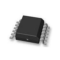
VN5050J-E STMicroelectronics, VN5050J-E Datasheet - Page 7

VN5050J-E
Manufacturer Part Number
VN5050J-E
Description
IC DRVR HIGHSIDE AUTO PWRSSO-12
Manufacturer
STMicroelectronics
Type
High Sider
Datasheet
1.VN5050JTR-E.pdf
(31 pages)
Specifications of VN5050J-E
Input Type
Non-Inverting
Number Of Outputs
1
On-state Resistance
50 mOhm
Current - Peak Output
19A
Voltage - Supply
4.5 V ~ 36 V
Operating Temperature
-40°C ~ 150°C
Mounting Type
Surface Mount
Package / Case
PowerSSO-12
Product
Driver ICs - Various
Supply Voltage (max)
36 V
Supply Voltage (min)
4.5 V
Supply Current
0.005 mA
Maximum Operating Temperature
+ 150 C
Mounting Style
SMD/SMT
Maximum Turn-off Delay Time
35000 ns
Maximum Turn-on Delay Time
20000 ns
Minimum Operating Temperature
- 40 C
Number Of Drivers
1
Device Type
High Side
Module Configuration
High Side
Peak Output Current
19A
Output Resistance
0.065ohm
Input Delay
20µs
Output Delay
35µs
Supply Voltage Range
4.5V To 36V
Rohs Compliant
Yes
Lead Free Status / RoHS Status
Lead free / RoHS Compliant
Current - Output / Channel
-
Lead Free Status / Rohs Status
Lead free / RoHS Compliant
Available stocks
Company
Part Number
Manufacturer
Quantity
Price
Part Number:
VN5050J-E
Manufacturer:
ST
Quantity:
20 000
VN5050J-E
2
Note:
2.1
Electrical specifications
Figure 3.
V
Absolute maximum ratings
Stressing the device above the rating listed in the “Absolute maximum ratings” table may
cause permanent damage to the device. These are stress ratings only and operation of the
device at these or any other conditions above those indicated in the Operating sections of
this specification is not implied. Exposure to the conditions in table below for extended
periods may affect device reliability. Refer also to the STMicroelectronics SURE Program
and other relevant quality document.
Table 4.
I
Symbol
STAT_DIS
F
- I
- I
- V
E
I
I
V
= V
STAT
OUT
I
MAX
GND
OUT
CC
IN
CC
OUT
DC supply voltage
Reverse DC supply voltage
DC reverse ground pin current
DC output current
Reverse DC output current
DC input current
DC status current
DC status disable current
Maximum switching energy
(L=3mH; R
- V
Current and voltage conventions
V
Absolute maximum ratings
SD
CC
V
during reverse battery condition.
IN
L
=0Ω; V
I
I
SD
IN
bat
=13.5V; T
STAT_DIS
INPUT
Parameter
jstart
GND
=150ºC; I
I
GND
OUTPUT
STATUS
V
CC
OUT
= I
limL
(Typ.))
I
OUT
I
STAT
Electrical specifications
V
STAT
Internally limited
V
V
OUT
+10 / -1
+10 / -1
+10 / -1
F
Value
I
200
104
0.3
S
41
12
V
CC
Unit
mA
mA
mA
mA
mJ
A
V
V
A
7/31


