VND5N07TR-E STMicroelectronics, VND5N07TR-E Datasheet - Page 8
VND5N07TR-E
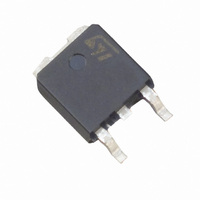
Manufacturer Part Number
VND5N07TR-E
Description
MOSFET OMNIFET 70V 5A DPAK
Manufacturer
STMicroelectronics
Series
OMNIFET II™r
Type
Low Sider
Datasheet
1.VND5N0713TR.pdf
(24 pages)
Specifications of VND5N07TR-E
Input Type
Non-Inverting
Number Of Outputs
1
On-state Resistance
200 mOhm
Current - Peak Output
5A
Mounting Type
Surface Mount
Package / Case
DPak, TO-252 (2 leads+tab), SC-63
Switch Type
Low Side
Power Switch Family
VND5N07
Input Voltage
18V
Power Switch On Resistance
200mOhm
Output Current
5A
Mounting
Surface Mount
Supply Current
250uA
Package Type
TO-252
Operating Temperature (min)
-40C
Operating Temperature (max)
150C
Operating Temperature Classification
Automotive
Pin Count
2 +Tab
Power Dissipation
60W
Lead Free Status / RoHS Status
Lead free / RoHS Compliant
Voltage - Supply
-
Operating Temperature
-
Current - Output / Channel
-
Lead Free Status / Rohs Status
Compliant
Available stocks
Company
Part Number
Manufacturer
Quantity
Price
Company:

Part Number:
VND5N07TR-E
Manufacturer:
INF
Quantity:
6 392
Part Number:
VND5N07TR-E
Manufacturer:
ST
Quantity:
20 000


Electrical specifications
8/24
Table 7.
1. Parameters guaranteed by design / characterization.
Table 8.
1. Pulsed: pulse duration = 300µs, duty cycle 1.5%.
2. Parameters guaranteed by design / characterization.
Table 9.
1. Parameters guaranteed by design / characterization.
Symbol
Symbol
Symbol
(dI/dt)
I
t
T
V
E
Q
RRM
dlim
T
t
t
t
t
I
t
jsh
d(on)
d(off)
d(on)
d(off)
SD
as
I
gf
rr
jrs
Q
rr
lim
t
t
t
t
(2)
r
r
(1)
f
f
(1)
i
(2)
(1)
(1)
(1)
(1)
(2)
on
Turn-on delay time
Rise time
Turn-off delay time
Fall time
Turn-on delay time
Rise time
Turn-off delay time
Fall time
Turn-on current slope
Total input charge
Forward On voltage
Reverse recovery time
Reverse recovery
charge
Reverse recovery
current
Drain current limit
Step response current
limit
Overtemperature
shutdown
Overtemperature reset
Fault sink current
Single pulse
avalanche energy
Switching
Source Drain diode
Protections (-40°C < T
Parameter
Parameter
Parameter
(1)
V
V
V
V
V
V
V
I
I
V
V
V
V
V
V
V
Starting T
V
SD
SD
DD
gen
DD
gen
DD
in
DD
DD
IN
IN
IN
IN
IN
IN
IN
= 10V; R
= 2.5A; V
= 2.5A; dI/dt = 100 A/µs
= 10V; V
= 5V; V
= 10V;
= 5V
= 10V; V
= 5V; V
= 10V R
j
= 15V; I
= 15V; I
= 15V; I
= 12V; I
= 30V;
= 10V; R
= 10V; R
< 150°C, unless otherwise specified)
Test conditions
Test conditions
Test conditions
j
= 25°C; V
DS
DS
gen
gen
D
D
D
D
DS
DS
IN
gen
gen
= 2.5A
= 2.5A
= 2.5A
= 2.5A; V
= 13V
= 13V
= 0V
= 10Ω
= 13V
= 13V;
= 1kΩ; L = 10mH
= 10Ω
= 1kΩ
DD
IN
= 20V
= 10V
Min.
Min.
Min.
150
135
3.5
3.5
0.2
3900
1100
Typ.
Typ.
Typ.
150
150
400
150
0.3
5.7
50
60
40
80
18
15
40
50
20
5
5
5000
1600
Max.
Max.
Max.
100
100
300
250
600
1.6
80
20
60
7
7
VND5N07
A/µS
Unit
Unit
Unit
mA
mA
nC
µC
µS
µS
ns
ns
ns
ns
ns
ns
ns
ns
ns
°C
°C
V
A
A
A
J
Related parts for VND5N07TR-E
Image
Part Number
Description
Manufacturer
Datasheet
Request
R

Part Number:
Description:
MOSFET N-CH 70V 5A DPAK
Manufacturer:
STMicroelectronics
Datasheet:

Part Number:
Description:
MOSFET Power N-Ch 70V 5A OmniFET
Manufacturer:
STMicroelectronics
Datasheet:

Part Number:
Description:
MOSFET OMNIFET 70V 5A IPAK
Manufacturer:
STMicroelectronics
Datasheet:
Part Number:
Description:
MOSFET PWR 70V 5A IPAK
Manufacturer:
STMicroelectronics
Datasheet:
Part Number:
Description:
STMicroelectronics [RIPPLE-CARRY BINARY COUNTER/DIVIDERS]
Manufacturer:
STMicroelectronics
Datasheet:
Part Number:
Description:
STMicroelectronics [LIQUID-CRYSTAL DISPLAY DRIVERS]
Manufacturer:
STMicroelectronics
Datasheet:

Part Number:
Description:
BOARD EVAL FOR MEMS SENSORS
Manufacturer:
STMicroelectronics
Datasheet:
Part Number:
Description:
NPN TRANSISTOR POWER MODULE
Manufacturer:
STMicroelectronics
Datasheet:
Part Number:
Description:
TURBOSWITCH ULTRA-FAST HIGH VOLTAGE DIODE
Manufacturer:
STMicroelectronics
Datasheet:
Part Number:
Description:
Manufacturer:
STMicroelectronics
Datasheet:
Part Number:
Description:
DIODE / SCR MODULE
Manufacturer:
STMicroelectronics
Datasheet:
Part Number:
Description:
DIODE / SCR MODULE
Manufacturer:
STMicroelectronics
Datasheet: