BUK215-50Y,118 NXP Semiconductors, BUK215-50Y,118 Datasheet - Page 6
BUK215-50Y,118
Manufacturer Part Number
BUK215-50Y,118
Description
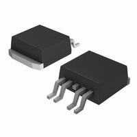
MOSFET N-CH 50V 9A SOT426
Manufacturer
NXP Semiconductors
Series
TOPFET™r
Type
High Sider
Datasheet
1.BUK215-50Y118.pdf
(13 pages)
Specifications of BUK215-50Y,118
Package / Case
D²Pak, TO-263 (4 leads + tab)
Input Type
Non-Inverting
Number Of Outputs
1
On-state Resistance
28 mOhm
Current - Output / Channel
9A
Current - Peak Output
45A
Voltage - Supply
5.5 V ~ 35 V
Mounting Type
Surface Mount
On Resistance (max)
0.038 Ohms
Maximum Power Dissipation
67000 mW
Mounting Style
SMD/SMT
Supply Current
2 mA
Switch Type
High Side
Power Switch Family
BUK215-50YT
Power Switch On Resistance
48mOhm
Output Current
9A
Mounting
Surface Mount
Package Type
D2PAK
Pin Count
4 +Tab
Power Dissipation
67W
Operating Temperature
-
Lead Free Status / RoHS Status
Lead free / RoHS Compliant
Operating Temperature
-
Lead Free Status / Rohs Status
Compliant
Other names
934055401118
BUK215-50Y /T3
BUK215-50Y /T3
BUK215-50Y /T3
BUK215-50Y /T3


Philips Semiconductors
OVERLOAD PROTECTION CHARACTERISTICS
5.5 V ≤ V
Refer to
SWITCHING CHARACTERISTICS
T
CAPACITANCES
T
1 The battery to load threshold voltage for short circuit protection is proportional to the battery supply voltage. After short circuit protection has
2 Measured from when the input goes high.
3 After cooling below the reset temperature the switch will resume normal operation.
May 2001
TOPFET high side switch
SMD version of BUK210-50Y
SYMBOL PARAMETER
I
V
t
T
∆T
mb
SYMBOL PARAMETER
t
dV/dt
t
t
dV/dt
t
mb
SYMBOL PARAMETER
C
C
C
L(lim)
d sc
d on
d off
on
off
j(TO)
BL(TO)
ig
bl
sg
= 25 ˚C, V
= 25 ˚C; f = 1 MHz; V
j(TO)
on
off
operated, the input voltage must be toggled low for the switch to resume normal operation.
TRUTH TABLE
BG
≤ 35 V, limits are at -40˚C ≤ T
Overload protection
Load current limiting
Short circuit load protection
Battery load threshold voltage
Response time
Overtemperature protection
Threshold junction
temperature
Hysteresis
During turn-on
Delay time
Rate of rise of load voltage
Total switching time
During turn-off
Delay time
Rate of fall of load voltage
Total switching time
Input capacitance
Output capacitance
Status capacitance
BG
= 13 V, for resistive load R
.
IG
3
= 0 V. designed in parameters.
2
mb
1
L
≤ 150˚C and typicals at T
= 13 Ω.
CONDITIONS
V
V
V
CONDITIONS
from input going high
to 10% V
30% to 70% V
to 90% V
from input going low
to 90% V
70% to 30% V
to 10% V
CONDITIONS
V
V
V
BL
BG
BL
BG
BL
SG
= V
> V
= 13 V
≥ 9 V
= 13 V
= 5 V
BG
BL(TO)
L
L
L
L
6
L
L
mb
V
V
= 25 ˚C unless otherwise stated.
BG
BG
= 16 V
= 35 V
MIN.
MIN.
MIN.
150
34
15
8
-
-
-
-
-
-
-
-
-
-
-
TYP.
TYP.
TYP.
0.35
180
170
140
250
0.6
45
10
20
10
40
55
85
15
11
Product specification
BUK215-50Y
MAX.
MAX.
MAX.
250
190
200
120
350
64
12
25
60
80
20
15
1
1
-
Rev 1.010
UNIT
UNIT
UNIT
V/µs
V/µs
µs
˚C
˚C
µs
µs
µs
µs
pF
pF
pF
A
V
V
Related parts for BUK215-50Y,118
Image
Part Number
Description
Manufacturer
Datasheet
Request
R

Part Number:
Description:
Manufacturer:
NXP Semiconductors
Datasheet:

Part Number:
Description:
Power Switch ICs - Power Distribution TAPE13 TOPFET2
Manufacturer:
NXP Semiconductors

Part Number:
Description:
TOPFET High Side Switch SMD Version
Manufacturer:
Philips Semiconductors
Datasheet:
Part Number:
Description:
NXP Semiconductors designed the LPC2420/2460 microcontroller around a 16-bit/32-bitARM7TDMI-S CPU core with real-time debug interfaces that include both JTAG andembedded trace
Manufacturer:
NXP Semiconductors
Datasheet:

Part Number:
Description:
NXP Semiconductors designed the LPC2458 microcontroller around a 16-bit/32-bitARM7TDMI-S CPU core with real-time debug interfaces that include both JTAG andembedded trace
Manufacturer:
NXP Semiconductors
Datasheet:
Part Number:
Description:
NXP Semiconductors designed the LPC2468 microcontroller around a 16-bit/32-bitARM7TDMI-S CPU core with real-time debug interfaces that include both JTAG andembedded trace
Manufacturer:
NXP Semiconductors
Datasheet:
Part Number:
Description:
NXP Semiconductors designed the LPC2470 microcontroller, powered by theARM7TDMI-S core, to be a highly integrated microcontroller for a wide range ofapplications that require advanced communications and high quality graphic displays
Manufacturer:
NXP Semiconductors
Datasheet:
Part Number:
Description:
NXP Semiconductors designed the LPC2478 microcontroller, powered by theARM7TDMI-S core, to be a highly integrated microcontroller for a wide range ofapplications that require advanced communications and high quality graphic displays
Manufacturer:
NXP Semiconductors
Datasheet:
Part Number:
Description:
The Philips Semiconductors XA (eXtended Architecture) family of 16-bit single-chip microcontrollers is powerful enough to easily handle the requirements of high performance embedded applications, yet inexpensive enough to compete in the market for hi
Manufacturer:
NXP Semiconductors
Datasheet:
Part Number:
Description:
The XA-S3 device is a member of Philips Semiconductors? XA(eXtended Architecture) family of high performance 16-bitsingle-chip microcontrollers
Manufacturer:
NXP Semiconductors
Datasheet:

Part Number:
Description:
The NXP BlueStreak LH75401/LH75411 family consists of two low-cost 16/32-bit System-on-Chip (SoC) devices
Manufacturer:
NXP Semiconductors
Datasheet:
Part Number:
Description:
The NXP LPC3130/3131 combine an 180 MHz ARM926EJ-S CPU core, high-speed USB2
Manufacturer:
NXP Semiconductors
Datasheet:
Part Number:
Description:
The NXP LPC3141 combine a 270 MHz ARM926EJ-S CPU core, High-speed USB 2
Manufacturer:
NXP Semiconductors
Part Number:
Description:
The NXP LPC3143 combine a 270 MHz ARM926EJ-S CPU core, High-speed USB 2
Manufacturer:
NXP Semiconductors