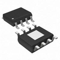
MAX256ASA+ Maxim Integrated Products, MAX256ASA+ Datasheet - Page 7

MAX256ASA+
Manufacturer Part Number
MAX256ASA+
Description
IC DVR H-BRIDGE 3W 8-SOIC
Manufacturer
Maxim Integrated Products
Type
H Bridger
Datasheet
1.MAX256ASA.pdf
(14 pages)
Specifications of MAX256ASA+
Input Type
Non-Inverting
Number Of Outputs
2
On-state Resistance
500 mOhm
Current - Output / Channel
600mA
Current - Peak Output
1A
Voltage - Supply
3 V ~ 5.5 V
Operating Temperature
-40°C ~ 125°C
Mounting Type
Surface Mount
Package / Case
8-SOIC (3.9mm Width) Exposed Pad, 8-eSOIC. 8-HSOIC
Supply Voltage (max)
5.5 V
Supply Voltage (min)
3 V
Maximum Operating Temperature
+ 125 C
Mounting Style
SMD/SMT
Maximum Power Dissipation
1509 mW
Minimum Operating Temperature
- 40 C
Supply Current
1.06 mA
Supply Voltage
5V
Digital Ic Case Style
SOIC
No. Of Pins
8
No. Of Regulated Outputs
2
Operating Temperature Range
-40°C To +125°C
Device Type
Half Bridge
Filter Terminals
SMD
Rohs Compliant
Yes
Lead Free Status / RoHS Status
Lead free / RoHS Compliant
Table 1. Oscillator Modes
With a supply voltage of +5V over the extended -40°C to
+85°C temperature range, the MAX256 is specified to
provide up to 3W of power to the primary side of a trans-
former in an isolated power supply. The device provides
up to 2.5W of power to the primary winding over the
+85°C to +125°C temperature range. The output power
is specified at ST1 and ST2 since losses in the trans-
former and rectification network are dependent upon
component selection and topology. The power dissipa-
tion of the MAX256 is approximated by:
where R
tance of the internal FET drivers, and I
current flowing through the transformer primary between
ST1 and ST2. For low output load currents, include the
contribution to P
I
As with all power-supply circuits, careful PC board lay-
out is important to achieve low switching losses and sta-
ble operation. For thermal performance, connect the
exposed paddle to a solid copper ground plane.
The traces from ST1 and ST2 to the transformer must be
low-resistance and inductance paths. Place the trans-
former as close as possible to the MAX256 using short,
wide traces.
When the device is operating with the internal oscillator,
it is possible for high-frequency switching components
on ST1 and ST2 to couple into the CK_RS circuitry
through PC board parasitic capacitance. This capacitive
CC
OSCILLATOR
Programmable
External Clock
x V
Frequency
Internal
Disable
3W Primary-Side Transformer H-Bridge Driver
MODE
CC
OHL
.
is the total high-side and low-side on-resis-
Applications Information
D
_______________________________________________________________________________________
P
from the quiescent supply current:
PC Board Layout Guidelines
Unconnected or pulled to ground by R
be greater than 10kΩ.
Digital input. Drive CK_RS with an external clock
signal.
Connected to V
(external clock mode)
Unconnected or pulled to ground with R
(internal clock mode)
D
=
R
Available Output Power
OHL
×
CC
I
PRI
or GND
2
CK_RS
PRI
is the load
S
. R
S
S
must
coupling can induce duty-cycle errors in the oscillator,
resulting in a DC current through the transformer. To
ensure proper operation, shield the CK_RS circuitry
from ST1 and ST2 by placing a grounded trace between
Figure 1. Secondary-Side Rectification Topologies
for Isolated Supplies
Ground
Ground
MODE
V
CC
V
V
V
+
-
+
-
+
-
IN
IN
IN
1:N CT
1:N
1:N
100kHz to 1MHz (typ).
Leave CK_RS unconnected for minimum
switching frequency.
CK_RS is pulled to ground by an internal
165kΩ resistor. The device switches at one
half the external clock frequency.
The device is disabled after a maximum of
55µs following the last rising edge on
CK_RS.
FIGURE 1A. PUSH-PULL RECTIFICATION
FIGURE 1B. VOLTAGE DOUBLER
FIGURE 1C. FULL-WAVE RECTIFIER
V
D =
OPERATION
DIODE FORWARD VOLTAGE
V
+
-
OUT =
N / 2 * V
IN -
V
+
+
V
-
-
OUT =
V
OUT =
D
2(NV
NV
IN -
IN -
2V
V
D
D
)
7


