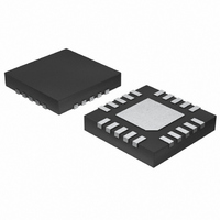
MAX4825ETP+ Maxim Integrated Products, MAX4825ETP+ Datasheet - Page 8

MAX4825ETP+
Manufacturer Part Number
MAX4825ETP+
Description
IC RELAY DRIVER 8CHAN 20-TQFN
Manufacturer
Maxim Integrated Products
Type
Relay/Lamp Driverr
Datasheet
1.MAX4823ETP.pdf
(19 pages)
Specifications of MAX4825ETP+
Input Type
Parallel
Number Of Outputs
8
On-state Resistance
2.7 Ohm
Current - Output / Channel
70mA
Current - Peak Output
150mA
Voltage - Supply
2.3 V ~ 5.5 V
Operating Temperature
-40°C ~ 85°C
Mounting Type
Surface Mount
Package / Case
20-TQFN Exposed Pad
Product
Relay Drivers
Rise Time
2 us
Fall Time
2 us
Supply Voltage (max)
5.5 V
Supply Voltage (min)
2.3 V
Supply Current
160 uA
Maximum Power Dissipation
1350 mW
Maximum Operating Temperature
- 40 C
Mounting Style
SMD/SMT
Minimum Operating Temperature
+ 85 C
Device Type
Relay
Output Current
70mA
Supply Voltage Range
2.3V To 5.5V
Driver Case Style
TQFN
No. Of Pins
20
Operating Temperature Range
-40°C To +85°C
Peak Reflow Compatible (260 C)
No
Rohs Compliant
Yes
Lead Free Status / RoHS Status
Lead free / RoHS Compliant
+3.3V/+5V, 8-Channel Relay Drivers with Fast
Recovery Time and Power-Save Mode
8
MAX4822
MAX4824
10, 16
_______________________________________________________________________________________
EP
19
20
11
12
1
2
3
4
5
6
7
8
9
PIN
PIN
MAX4823
MAX4825
10, 16
EP
19
20
11
12
1
2
3
4
5
6
7
8
9
NAME
NAME
RESET
PGND
OUT8
OUT7
OUT6
OUT5
GND
V
SET
LVL
CS
EP
A0
A1
A2
CC
Input Supply Voltage. Bypass V
Set Input. Drive SET low to set all latches and registers high (all outputs are low
impedance). SET overrides all parallel and serial control inputs. RESET overrides SET
under all conditions.
Exposed Pad. Connect exposed paddle to GND.
Reset Input. Drive RESET low to clear all latches and registers (all outputs are high
impedance). RESET overrides all other inputs. If RESET and SET are pulled low at the
same time, then RESET takes precedence.
Chip-Select Input. Drive CS low to select the device. The CS falling edge latches the
output address (A0, A1, A2). The CS rising edge latches level data (LVL).
Level Input. LVL determines whether the selected address is switched on or off. Logic-
high on LVL switches on the addressed output. A logic-low on LVL switches off the
addressed output.
Digital Address 0 Input. (See Figure 3 for address mapping.)
Digital Address 1 Input. (See Figure 3 for address mapping.)
Digital Address 2 Input. (See Figure 3 for address mapping.)
Ground
Open-Drain Output 8. Connect OUT8 to the low side of a relay coil. This output is pulled
to PGND when activated, but otherwise is high impedance.
Open-Drain Output 7. Connect OUT7 to the low side of a relay coil. This output is pulled
to PGND when activated, but otherwise is high impedance.
Power Ground. PGND is a return for the output sinks. Connect PGND pins together and
to GND.
Open-Drain Output 6. Connect OUT6 to the low side of a relay coil. This output is pulled
to PGND when activated, but otherwise is high impedance.
Open-Drain Output 5. Connect OUT5 to the low side of a relay coil. This output is pulled
to PGND when activated, but otherwise is high impedance.
MAX4822/MAX4823 Pin Description (continued)
MAX4824/MAX4825 Pin Description
CC
to GND with a 0.1µF capacitor.
FUNCTION
FUNCTION


