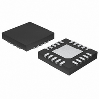
MAX4825ETP+ Maxim Integrated Products, MAX4825ETP+ Datasheet - Page 4

MAX4825ETP+
Manufacturer Part Number
MAX4825ETP+
Description
IC RELAY DRIVER 8CHAN 20-TQFN
Manufacturer
Maxim Integrated Products
Type
Relay/Lamp Driverr
Datasheet
1.MAX4823ETP.pdf
(19 pages)
Specifications of MAX4825ETP+
Input Type
Parallel
Number Of Outputs
8
On-state Resistance
2.7 Ohm
Current - Output / Channel
70mA
Current - Peak Output
150mA
Voltage - Supply
2.3 V ~ 5.5 V
Operating Temperature
-40°C ~ 85°C
Mounting Type
Surface Mount
Package / Case
20-TQFN Exposed Pad
Product
Relay Drivers
Rise Time
2 us
Fall Time
2 us
Supply Voltage (max)
5.5 V
Supply Voltage (min)
2.3 V
Supply Current
160 uA
Maximum Power Dissipation
1350 mW
Maximum Operating Temperature
- 40 C
Mounting Style
SMD/SMT
Minimum Operating Temperature
+ 85 C
Device Type
Relay
Output Current
70mA
Supply Voltage Range
2.3V To 5.5V
Driver Case Style
TQFN
No. Of Pins
20
Operating Temperature Range
-40°C To +85°C
Peak Reflow Compatible (260 C)
No
Rohs Compliant
Yes
Lead Free Status / RoHS Status
Lead free / RoHS Compliant
+3.3V/+5V, 8-Channel Relay Drivers with Fast
Recovery Time and Power-Save Mode
ELECTRICAL CHARACTERISTICS (continued)
(V
noted.) (Note 1)
4
Note 1: Specifications at -40°C are guaranteed by design and not production tested.
Note 2: Thermal shutdown disables power save from all channels to reduce power dissipation inside the device.
Note 3: Thermal shutdown turns off all channels.
Note 4: The circuit can set the output voltage in power-save mode only if I
Note 5: After relay turn-off, inductive kickback can momentarily cause the OUT_ voltage to exceed V
Note 6: Guaranteed by design.
Note 7: For other capacitance values, use the equation t
Data Hold Time
SCLK Fall to DOUT Valid
Rise Time (DIN, SCLK, CS, SET,
RESET)
Fall Time (DIN, SCLK, CS,
RESET, SET)
RESET Minimum Pulse Width
SET Minimum Pulse Width
CS Minimum Pulse Width
PARALLEL TIMING (MAX4824/MAX4825)
Turn-On Time
Turn-Off Time
LVL Setup Time
LVL Hold Time
Address to CS Setup Time
Address to CS Hold Time
Rise Time (A2, A1, A0, LVL)
Fall Time (A2, A1, A0, LVL)
RESET Pulse Width
SET Pulse Width
CS Minimum Pulse Width
POWER-SAVE TIMING (MAX4822/MAX4824)
Power-Save Delay Time
Minimum PSAVE Low Time to
Power-Save Reset
CC
_______________________________________________________________________________________
= +2.7V to +5.5V, T
normal operation and does not damage the device.
PARAMETER
A
= -40°C to +85°C, unless otherwise noted. Typical values are at V
SYMBOL
t
t
t
t
t
t
t
t
t
t
t
CSW
t
t
t
CSW
t
SCR
t
SCR
SCF
OFF
t
t
SCF
t
PSR
t
DH
DO
RW
SW
ON
RW
SW
LH
AS
AH
LS
PS
50% of SCLK to (V
C
20% of V
(Note 6)
20% of V
(Note 6)
From rising edge of CS, R
C
From rising edge of CS, R
C
20% of V
(Note 6)
20% of V
(Note 6)
Variation from typical value, C
(Note 7)
L
L
L
= 50pF
= 50pF
= 50pF
PS
CC
CC
CC
CC
= 32 x C.
to 70% of V
to 70% of V
to 70% of V
to 70% of V
CONDITIONS
IH
, V
IL
CC
CC
CC
CC
OUT
of D
L
L
, C
, C
, C
, C
= 50 ,
= 50 ,
IN
L
L
L
L
x R
L
= 50pF
= 50pF
= 50pF
= 50pF
),
= 100nF
ON
< V
OUTP
CC
.
= 2.7V, T
MIN
1.6
70
70
40
20
20
70
70
40
0
0
0
CC
. This is considered part of
A
= +25°C, unless otherwise
TYP
3.2
17
2
MAX
5.4
3.5
28
2
2
1
3
2
2
UNITS
ms
ms
ns
ns
µs
µs
ns
ns
ns
µs
µs
ns
ns
ns
ns
µs
µs
ns
ns
ns


