NUD3112DMT1G ON Semiconductor, NUD3112DMT1G Datasheet - Page 2
NUD3112DMT1G
Manufacturer Part Number
NUD3112DMT1G
Description
MOSFT N-CH DUAL 14V 500MA SC74-6
Manufacturer
ON Semiconductor
Type
Low Sider
Datasheet
1.NUD3112LT1G.pdf
(7 pages)
Specifications of NUD3112DMT1G
Input Type
Non-Inverting
Number Of Outputs
2
On-state Resistance
1.2 Ohm
Current - Output / Channel
400mA
Current - Peak Output
500mA
Operating Temperature
-40°C ~ 85°C
Mounting Type
Surface Mount
Package / Case
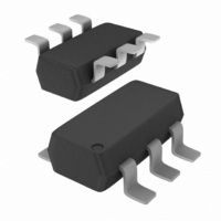
SC-74-6
Configuration
Dual
Transistor Polarity
N-Channel
Resistance Drain-source Rds (on)
0.9 Ohm @ 5 V
Drain-source Breakdown Voltage
14 V
Gate-source Breakdown Voltage
6 V
Continuous Drain Current
0.5 A
Power Dissipation
380 mW
Maximum Operating Temperature
+ 85 C
Mounting Style
SMD/SMT
Minimum Operating Temperature
- 40 C
Supply Voltage Max
14V
No. Of Outputs
2
Output Voltage
14V
Output Current
400mA
Driver Case Style
SC-74
Device Type
Relay
Termination Type
SMD
No. Of Pins
6
Rohs Compliant
Yes
Filter Terminals
SMD
Leaded Process Compatible
Yes
Lead Free Status / RoHS Status
Lead free / RoHS Compliant
Voltage - Supply
-
Lead Free Status / Rohs Status
Lead free / RoHS Compliant
Other names
NUD3112DMT1GOS
NUD3112DMT1GOS
NUD3112DMT1GOSTR
NUD3112DMT1GOS
NUD3112DMT1GOSTR
Available stocks
Company
Part Number
Manufacturer
Quantity
Price
Company:

Part Number:
NUD3112DMT1G
Manufacturer:
ON
Quantity:
6 000
Part Number:
NUD3112DMT1G
Manufacturer:
ON/安森美
Quantity:
20 000


1. Mounted onto minimum pad board.
MAXIMUM RATINGS
TYPICAL ELECTRICAL CHARACTERISTICS
OFF CHARACTERISTICS
ON CHARACTERISTICS
Symbol
Symbol
V
R
V
B
I
V
DS(on)
R
ESD
BRDSS
I
I
V
GS(th)
DS(on)
T
VGSO
g
GSS
DSS
P
P
DSS
E
T
T
I
stg
qJA
GS
FS
D
A
D
D
z
J
Drain to Source Voltage – Continuous
Gate to Source Voltage – Continuous
Drain Current – Continuous
Single Pulse Drain−to−Source Avalanche Energy (
Junction Temperature
Operating Ambient Temperature
Storage Temperature Range
Total Power Dissipation (Note 1)
Derating Above 25°C
Total Power Dissipation (Note 1)
Derating Above 25°C
Thermal Resistance Junction−to−Ambient (Note 1)
Human Body Model (HBM) According to EIA/JESD22/A114
Drain to Source Sustaining Voltage (Internally Clamped)
I
Drain to Source Leakage Current
Gate Body Leakage Current
Gate Threshold Voltage
Drain to Source On−Resistance
Output Continuous Current
Forward Transconductance
g
(I D = 10 mA)
= 1.0 mA
(V
(V
(V
(V
(V
(V
(I
(I
(I
(I
(I
(V
(V
(V
D
D
D
D
D
DS
DS
GS
GS
GS
GS
DS
DS
OUT
= 250 mA, V
= 500 mA, V
= 500 mA, V
= 500 mA, V
= 500 mA, V
= 12 V , V
= 12 V, V
= 0.25 V, V
= 0.25 V, V
= 3.0 V, V
= 5.0 V, V
= V
= V
= 12.0 V, I
(T
DS
DS
J
= 25°C unless otherwise specified)
, I
, I
D
D
GS
DS
DS
= 1.0 mA)
= 1.0 mA, T
GS
GS
GS
GS
GS
GS
GS
GS
OUT
= 0 V, T
= 0 V)
= 0 V)
= 0 V, T
= 3.0 V)
= 3.0 V)
= 5.0 V)
= 3.0 V, T
= 5.0 V, T
= 3.0 V)
= 3.0 V, T
= 0.25 A)
A
A
A
= 85°C)
= 25°C)
A
A
Characteristic
= 85°C)
A
=85°C)
=85°C)
= 85°C)
(T
A
= 25°C unless otherwise noted)
http://onsemi.com
Rating
T
Jinitial =
2
25°C)
Min
300
200
350
0.8
0.8
14
−
−
−
−
−
−
−
−
−
−
SOT−23
SOT−23
SC−74
SC−74
Typ
400
490
1.2
16
−
−
−
−
−
−
−
−
−
−
−
−
−65 to +150
−40 to 85
Value
2000
500
150
225
380
556
329
1.8
3.0
14
50
6
Max
1.4
1.4
1.2
1.3
0.9
1.3
0.9
17
20
40
35
65
8
−
−
−
mW/°C
mW/°C
mmhos
°C/W
Unit
Unit
mW
mW
V
V
mA
mA
mJ
°C
°C
°C
mA
mA
W
V
V
V
V
dc
dc
Related parts for NUD3112DMT1G
Image
Part Number
Description
Manufacturer
Datasheet
Request
R

Part Number:
Description:
ON Semiconductor [VOLTAGE REGULATOR]
Manufacturer:
ON Semiconductor
Datasheet:
Part Number:
Description:
357-036-542-201 CARDEDGE 36POS DL .156 BLK LOPRO
Manufacturer:
ON Semiconductor
Datasheet:
Part Number:
Description:
357-036-542-201 CARDEDGE 36POS DL .156 BLK LOPRO
Manufacturer:
ON Semiconductor
Datasheet:
Part Number:
Description:
357-036-542-201 CARDEDGE 36POS DL .156 BLK LOPRO
Manufacturer:
ON Semiconductor
Datasheet:
Part Number:
Description:
357-036-542-201 CARDEDGE 36POS DL .156 BLK LOPRO
Manufacturer:
ON Semiconductor
Datasheet:
Part Number:
Description:
357-036-542-201 CARDEDGE 36POS DL .156 BLK LOPRO
Manufacturer:
ON Semiconductor
Datasheet:
Part Number:
Description:
357-036-542-201 CARDEDGE 36POS DL .156 BLK LOPRO
Manufacturer:
ON Semiconductor
Datasheet:
Part Number:
Description:
357-036-542-201 CARDEDGE 36POS DL .156 BLK LOPRO
Manufacturer:
ON Semiconductor
Datasheet:
Part Number:
Description:
357-036-542-201 CARDEDGE 36POS DL .156 BLK LOPRO
Manufacturer:
ON Semiconductor
Datasheet:
Part Number:
Description:
357-036-542-201 CARDEDGE 36POS DL .156 BLK LOPRO
Manufacturer:
ON Semiconductor
Datasheet:
Part Number:
Description:
357-036-542-201 CARDEDGE 36POS DL .156 BLK LOPRO
Manufacturer:
ON Semiconductor
Datasheet:
Part Number:
Description:
Manufacturer:
ON Semiconductor
Datasheet:
Part Number:
Description:
Manufacturer:
ON Semiconductor
Datasheet: