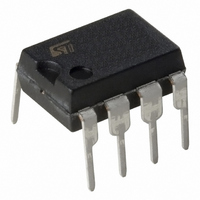
TDE1798DP STMicroelectronics, TDE1798DP Datasheet - Page 3

TDE1798DP
Manufacturer Part Number
TDE1798DP
Description
IC SWITCH .5A INTEL PWR 8MINIDIP
Manufacturer
STMicroelectronics
Type
High Sider
Datasheet
1.TDE1798DP.pdf
(14 pages)
Specifications of TDE1798DP
Input Type
Differential
Number Of Outputs
1
Current - Output / Channel
500mA
Current - Peak Output
900mA
Voltage - Supply
6 V ~ 35 V
Operating Temperature
-25°C ~ 85°C
Mounting Type
Through Hole
Package / Case
8-DIP (0.200", 5.08mm)
Maximum Operating Temperature
+ 150 C
Minimum Operating Temperature
- 65 C
Mounting Style
Through Hole
Supply Current
8 mA
Supply Voltage Min
6V
Supply Voltage Max
35V
No. Of Outputs
1
Output Voltage
1V
Output Current
500mA
Driver Case Style
DIP
Leaded Process Compatible
Yes
No. Of Pins
8
Rohs Compliant
Yes
Lead Free Status / RoHS Status
Lead free / RoHS Compliant
On-state Resistance
-
Lead Free Status / Rohs Status
Lead free / RoHS Compliant
Other names
497-2184-5
Available stocks
Company
Part Number
Manufacturer
Quantity
Price
Company:
Part Number:
TDE1798DP
Manufacturer:
ST
Quantity:
5 216
Part Number:
TDE1798DP
Manufacturer:
ST
Quantity:
20 000
THERMAL DATA
1) Devices bounded on a 40cm
ELECTRICAL CHARACTERISTICS (note 2)
TDE -25 C
Notes:
2) For operating at high temperature, the TDE1798 must be derated based on a 150 C maximum junction temperature and the junction-ambient
thermal resistance.
3) The offset voltage given is the maximum value of input differential voltage required to drive the output voltage within 2V of the ground or the
supply voltage;
4) Input voltage range is independent of the supply voltage;
5) The reference input can be the inverting or the non-inverting one.
I
R
I
OL(open GND)
Symbol
(pin 1) source
R
V
I
Symbol
th j-ambient
(pin 6) sink
V
CC
th j-case
V
I
BRVEO
V
I
I
I
I
V
reset
I
I
V
CC
SC
RH
OL
RL
ICR
IB
IO
th
- V
I
O
Thermal Resistance Junction-case (1)
Thermal Resistance Junction-ambient (1)
Input Offset Voltage
Power Supply Current
Input Bias Current
Common-mode Input Voltage
Range
Input Voltage Range
Short-circuit Output Current
Output Saturation Voltage
Output Low Leakage Current
Available Alarm Output Current
Reset Input Current
Reset Threshold
Reset Output Sink Current
Output Leakage Current
Output Transistor Avalanche Volt. V
T
j
+85 C, 6V
Parameter
2
glass-epoxy printed circuit 0.15cm thick with 4cm
V
CC
+35V, I
Description
(note 3)
Output High (Tamb = +25 C,
I
Output Low
(note 4)
V
V
I
T
Source (V
Sink (in thermal shut-down)
V
(in thermal shut-down) for
V
(open ground)
o
O
o
j
(pin 6)
ref
CC
reset
CC
= 500mA)
= +85 C (V
= 500mA (|V
> +1V, (note 4 and 5)
= 30V, t = 10ms
- V
500mA (unless otherwise specified).
= 2V
O
+0.8V
Test Condition
(pin 1)
CC
= V
+
= 30V, V
I - V
CC
2
of copper
-
- 2.5V)
I|> 50mV)
O
= 0V)
Min.
-25
0.7
0.8
65
-1
–
–
–
–
1
–
–
4
6
–
2
–
max.
max.
Typ.
6.5
0.9
1.4
15
10
15
15
10
2
2
–
–
1
8
0
–
–
Value
30
90
Max.
1.25
100
100
110
1.3
50
40
45
45
40
+1
8
4
–
–
2
–
TDE1798
Unit
Unit
C/W
C/W
mV
mA
mA
mA
mA
mA
V
A
V
V
V
V
A
A
A
A
A
3/14


