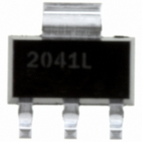
IPS2041LPBF International Rectifier, IPS2041LPBF Datasheet - Page 3

IPS2041LPBF
Manufacturer Part Number
IPS2041LPBF
Description
INTELLIGENT POWER SW 1CH SOT223
Manufacturer
International Rectifier
Type
Low Sider
Specifications of IPS2041LPBF
Input Type
Non-Inverting
Number Of Outputs
1
On-state Resistance
100 mOhm
Current - Output / Channel
1.4A
Current - Peak Output
5.5A
Voltage - Supply
4 V ~ 5.5 V
Operating Temperature
-40°C ~ 150°C
Mounting Type
Surface Mount
Package / Case
SOT-223 (3 leads + Tab), SC-73, TO-261
Current, Leakage, Offset
50 μA
Current, Supply
4 mA
Package Type
SOT-223
Polarization
N-Channel
Power Dissipation
1.6 W
Resistance, Drain To Source On
130 Milliohms
Temperature, Operating, Maximum
+150 °C
Temperature, Operating, Minimum
–40 °C
Time, Turn-off Delay
425 ns
Time, Turn-on Delay
675 ns
Voltage, Supply
39 V
Power Load Switch Type
Low Side
Input Voltage
5.5V
Current Limit
1.4A
On State Resistance
0.1ohm
Thermal Protection
Yes
On / Enable Input Polarity
Active Low
Power Dissipation Pd
1W
No. Of Outputs
1
Rohs Compliant
Yes
Lead Free Status / RoHS Status
Lead free / RoHS Compliant
Available stocks
Company
Part Number
Manufacturer
Quantity
Price
Company:
Part Number:
IPS2041LPBF
Manufacturer:
IR
Quantity:
12 500
NOTE: For high side PWM, HIN pulse width must be
Dynamic Electrical Characteristics
V
electrical characteristics are defined in Figures 3 through 5.
Static Electrical Characteristics
V
are referenced to V
are referenced to V
www.irf.com
Symbol
Symbol
BIAS
BIAS
V
V
V
R
V
V
I
I
SR+
ITRIP+
I
ITRIP-
CCUV+
t
t
I
BSUV+
SR-
V
CCUV-
t
IT,TH+
V
BSUV-
on,FLT
DT
QCC
I
fltclr
V
QBS
t
t
flt,in
V
I
I
itrip
t
t
IN+
on
off
t
IN-
t
flt
OH
LK
bl
OL
r
f
IH
IL
(V
(V
CC
CC
, V
, V
Turn-On Propagation Delay
Turn-Off Propagation Delay
Turn-On Rise Time
Turn-Off Fall Time
ITRIP to Output Shutdown Prop. Delay
ITRIP Blanking Time
ITRIP to
Input Filter Time (All Six Inputs)
Deadtime
Operational Amplifier Slew Rate (+)
Operational Amplifier Slew Rate (-)
BS1,2,3
BS1,2,3
LIN1,2,3
Logic “0” Input Voltage (OUT = LO)
Logic “1” Input Voltage (OUT = HI)
ITRIP Input Positive Going Threshold
High Level Output Voltage, V
Low Level Output Voltage, V
Offset Supply Leakage Current
Quiescent V
Quiescent V
Logic “1” Input Bias Current (OUT = HI)
Logic “0” Input Bias Current (OUT = LO)
“High” ITRIP Bias Current
“Low” ITRIP Bias Current
V
Threshold
V
Threshold
V
Threshold
V
Threshold
FAULT
BS
BS
CC
CC
Supply Undervoltage Positive Going
Supply Undervoltage Negative Going
SS
S0,1,2,3
Supply Undervoltage Positive Going
Supply Undervoltage Negative Going
) = 15V, V
) = 15V, V
Low On-Resistance
and are applicable to all six logic input leads:
FAULT
to
FAULT
BS
CC
and are applicable to the respective output leads: HO1,2,3 or LO1,2,3.
Definition
(IR2130)
(IR2132)
Definition
Supply Current
Supply Current
Indication Delay
S0,1,2,3
S0,1,2,3
Clear Time
= V
= V
SS
O
SS
BIAS
, C
and T
- V
L
= 1000 pF and T
O
A
= 25°C unless otherwise specified. The V
IR2130/IR2132(J)(S) & (PbF)
Figure Min. Typ. Max. Units Test Conditions
Figure Min. Typ. Max. Units Test Conditions
sec
11
12
13
14
15
16
17
18
18
19
20
—
—
21
22
23
24
25
26
27
28
29
30
31
32
33
34
35
36
37
A
HIN1,2,3
= 25°C unless otherwise specified. The dynamic
500
300
400
335
400
6.0
1.3
0.4
4.4
2.4
2.2
7.5
7.1
8.3
8.0
—
—
—
—
—
—
—
—
—
—
—
—
—
—
—
8.35
7.95
675
425
660
400
590
310
225
9.0
2.5
0.8
6.2
3.2
490
450
&
3.0
9.0
8.7
80
35
—
—
—
—
—
15
75
—
55
LIN1,2,3
12.0
850
550
125
920
845
3.7
1.2
580
100
100
650
400
150
100
55
—
—
—
—
0.8
4.0
9.2
8.8
9.7
9.4
50
30
75
—
. The V
V/µs
µA
mV
mA
ns
µA
nA
µs
IN
V
V
, V
O
TH
and I
V
V
V
V
IN
IN
IN
V
V
and I
S1,2,3
V
V
V
IN
IN
, V
, V
, V
V
O
V
V
B
V
IN
IN
ITRIP = 5V
ITRIP = 0V
IN
IN
IN
= 0V, I
= 5V, I
= V
ITRIP
parameters
V
V
ITRIP
ITRIP
ITRIP
IN
= 0V or 5V
= 0V or 5V
= 0 & 5V
IN
IN
= 0 & 5V
= 0 & 5V
= 0 to 600V
S
parameters
= 0V
= 5V
= 600V
= 1V
= 0 & 5V
= 0 & 5V
= 0 & 5V
O
O
= 0A
= 0A
3


