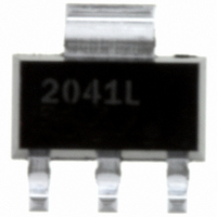
IPS2041LPBF International Rectifier, IPS2041LPBF Datasheet - Page 2

IPS2041LPBF
Manufacturer Part Number
IPS2041LPBF
Description
INTELLIGENT POWER SW 1CH SOT223
Manufacturer
International Rectifier
Type
Low Sider
Specifications of IPS2041LPBF
Input Type
Non-Inverting
Number Of Outputs
1
On-state Resistance
100 mOhm
Current - Output / Channel
1.4A
Current - Peak Output
5.5A
Voltage - Supply
4 V ~ 5.5 V
Operating Temperature
-40°C ~ 150°C
Mounting Type
Surface Mount
Package / Case
SOT-223 (3 leads + Tab), SC-73, TO-261
Current, Leakage, Offset
50 μA
Current, Supply
4 mA
Package Type
SOT-223
Polarization
N-Channel
Power Dissipation
1.6 W
Resistance, Drain To Source On
130 Milliohms
Temperature, Operating, Maximum
+150 °C
Temperature, Operating, Minimum
–40 °C
Time, Turn-off Delay
425 ns
Time, Turn-on Delay
675 ns
Voltage, Supply
39 V
Power Load Switch Type
Low Side
Input Voltage
5.5V
Current Limit
1.4A
On State Resistance
0.1ohm
Thermal Protection
Yes
On / Enable Input Polarity
Active Low
Power Dissipation Pd
1W
No. Of Outputs
1
Rohs Compliant
Yes
Lead Free Status / RoHS Status
Lead free / RoHS Compliant
Available stocks
Company
Part Number
Manufacturer
Quantity
Price
Company:
Part Number:
IPS2041LPBF
Manufacturer:
IR
Quantity:
12 500
Note 1: Logic operational for V
(Please refer to the Design Tip DT97-3 for more details).
Note 2: All input pins, CA- and CAO pins are internally clamped with a 5.2V zener diode.
Absolute Maximum Ratings
Absolute Maximum Ratings indicate sustained limits beyond which damage to the device may occur. All voltage param-
eters are absolute voltages referenced to V
under board mounted and still air conditions. Additional information is shown in Figures 50 through 53.
IR2130/IR2132(J)(S) & (PbF)
Recommended Operating Conditions
The Input/Output logic timing diagram is shown in Figure 1. For proper operation the device should be used within the
recommended conditions. All voltage parameters are absolute voltages referenced to V
with all supplies biased at 15V differential. Typical ratings at other bias conditions are shown in Figure 54.
Symbol
Symbol
2
V
V
V
V
V
V
dV
V
V
Rth
HO1,2,3
V
LO1,2,3
V
V
V
HO1,2,3
LO1,2,3
V
V
B1,2,3
S1,2,3
V
V
V
V
B1,2,3
S1,2,3
V
P
V
T
CAO
T
T
CAO
T
FLT
CA-
CC
FLT
CA-
SS
S
IN
CC
SS
D
S
L
IN
J
A
/dt
JA
High Side Floating Supply Voltage
High Side Floating Offset Voltage
High Side Floating Output Voltage
Low Side and Logic Fixed Supply Voltage
Logic Ground
Low Side Output Voltage
Logic Input Voltage (
Operational Amplifier Output Voltage
Operational Amplifier Inverting Input Voltage
Allowable Offset Supply Voltage Transient
Package Power Dissipation @ T
Thermal Resistance, Junction to Ambient
Junction Temperature
Storage Temperature
Lead Temperature (Soldering, 10 seconds)
FAULT
High Side Floating Supply Voltage
High Side Floating Offset Voltage
High Side Floating Output Voltage
Low Side and Logic Fixed Supply Voltage
Logic Ground
Low Side Output Voltage
Logic Input Voltage (
Operational Amplifier Output Voltage
Operational Amplifier Inverting Input Voltage
Ambient Temperature
FAULT
Output Voltage
Output Voltage
S
of (V
HIN1,2,3
S0
HIN1,2,3
- 5V) to (V
Definition
Definition
S0
,
. The Thermal Resistance and Power Dissipation ratings are measured
,
LIN1,2,3
A
LIN1,2,3
S0
+25°C
+ 600V). Logic state held for V
& ITRIP)
& ITRIP)
(44 Lead PLCC)
(44 Lead PLCC)
(28 Lead SOIC)
(28 Lead SOIC)
(28 Lead DIP)
(28 Lead DIP)
V
V
V
V
V
V
V
S1,2,3
V
B1,2,3
S
S1,2,3
SS
Note 1
V
SS
SS
SS
Min.
CC
Min.
of (V
-0.3
-0.3
-0.3
S0
V
V
V
V
-55
S1,2,3
-40
—
—
—
—
—
—
—
—
—
10
-5
0
SS
SS
SS
SS
- 0.3
- 0.3
- 0.3
- 0.3
- 25
. The V
- 0.3
- 25
+ 10
S0
- 5V) to (V
S
(V
V
V
whichever is
(V
offset rating is tested
V
V
V
V
V
V
B1,2,3
B1,2,3
SS
S1,2,3
V
V
V
CC
CC
CC
CC
CC
CC
Max.
V
Max.
lower
SS
SS
SS
625
150
150
300
V
V
1.5
1.6
2.0
600
B1,2,3
125
25
+ 15) or
50
83
78
63
20
5
+ 0.3
+ 0.3
+ 0.3)
+ 0.3
+ 0.3
+ 0.3
CC
CC
S0
+ 0.3
+ 5
+ 5
+ 5
+ 0.3
+ 20
- V
www.irf.com
BS
).
Units
Units
°C/W
°C
V/ns
V
W
°C
V


