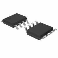
BD2061AFJ-E2 Rohm Semiconductor, BD2061AFJ-E2 Datasheet - Page 8

BD2061AFJ-E2
Manufacturer Part Number
BD2061AFJ-E2
Description
IC SWITCH USB HI SIDE 1CH SOP-J8
Manufacturer
Rohm Semiconductor
Type
High Sider
Specifications of BD2061AFJ-E2
Input Type
Non-Inverting
Number Of Outputs
1
On-state Resistance
80 mOhm
Current - Output / Channel
1A
Current - Peak Output
1.5A
Voltage - Supply
2.7 V ~ 5.5 V
Operating Temperature
-40°C ~ 85°C
Mounting Type
Surface Mount
Package / Case
8-SOPJ
Primary Input Voltage
5V
No. Of Outputs
1
Output Voltage
5V
Output Current
1A
Voltage Regulator Case Style
SOP
No. Of Pins
8
Operating Temperature Range
-40°C To +85°C
Svhc
No SVHC
Output Power
560 mW
Input Voltage
2.7 V to 5.5 V
Mounting Style
SMD/SMT
Lead Free Status / RoHS Status
Lead free / RoHS Compliant
Lead Free Status / RoHS Status
Lead free / RoHS Compliant, Lead free / RoHS Compliant
Other names
BD2061AFJ-E2TR
Available stocks
Company
Part Number
Manufacturer
Quantity
Price
Company:
Part Number:
BD2061AFJ-E2
Manufacturer:
PANASONIC
Quantity:
38
Part Number:
BD2061AFJ-E2
Manufacturer:
ROHM/罗姆
Quantity:
20 000
●I/O circuit
●Functional description
© 2011 ROHM Co., Ltd. All rights reserved.
BD2061AFJ,BD2065AFJ
www.rohm.com
1. Switch operation
2. Thermal shutdown circuit (TSD)
3. Over current detection (OCD)
IN terminal and OUT terminal are connected to the drain and the source of switch MOSFET respectively. And the IN
terminal is used also as power source input to internal control circuit.
When the switch is turned on from EN/EN control input, IN terminal and OUT terminal are connected by a 80mΩ switch. In
on status, the switch is bidirectional. Therefore, when the potential of OUT terminal is higher than that of IN terminal,
current flows from OUT terminal to IN terminal.
Since a parasitic diode between the drain and the source of switch MOSFET is canceled, in the off status, it is possible to
prevent current from flowing reversely from OUT to IN.
If over current would continue, the temperature of the IC would increase drastically. If the junction temperature were
beyond 140℃ (typ.) in the condition of over current detection, thermal shutdown circuit operates and makes power switch
turn off and outputs error flag (/OC). Then, when the junction temperature decreases lower than 120℃ (typ.), power
switch is turned on and error flag (/OC) is cancelled. Unless the fact of the increasing chips temperature is removed or the
output of power switch is turned off, this operation repeats.
The thermal shutdown circuit operates when the switch is on (EN,/EN signal is active).
The over current detection circuit limits current (I
MOSFET exceeds a specified value. There are three types of response against over current. The over current detection
circuit works when the switch is on (EN,/EN signal is active).
3-1. When the switch is turned on while the output is in shortcircuit status
3-2. When the output shortcircuits while the switch is on
3-3. When the output current increases gradually
EN(/EN)
Symbol
OUT
When the switch is turned on while the output is in shortcircuit status or so, the switch gets in current limit status soon.
When the output shortcircuits or large capacity is connected while the switch is on, very large current flows until the
over current limit circuit reacts. When the current detection, limit circuit works, current limitation is carried out.
When the output current increases gradually, current limitation does not work until the output current exceeds the over
current detection value. When it exceeds the detection value, current limitation is carried out.
/OC
Pin No
6,7,8
4
5
SC
) and outputs error flag (/OC) when current flowing in each switch
8/12
Equivalent circuit
Technical Note
2011.03 - Rev.B


