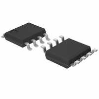
BD2061AFJ-E2 Rohm Semiconductor, BD2061AFJ-E2 Datasheet - Page 10

BD2061AFJ-E2
Manufacturer Part Number
BD2061AFJ-E2
Description
IC SWITCH USB HI SIDE 1CH SOP-J8
Manufacturer
Rohm Semiconductor
Type
High Sider
Specifications of BD2061AFJ-E2
Input Type
Non-Inverting
Number Of Outputs
1
On-state Resistance
80 mOhm
Current - Output / Channel
1A
Current - Peak Output
1.5A
Voltage - Supply
2.7 V ~ 5.5 V
Operating Temperature
-40°C ~ 85°C
Mounting Type
Surface Mount
Package / Case
8-SOPJ
Primary Input Voltage
5V
No. Of Outputs
1
Output Voltage
5V
Output Current
1A
Voltage Regulator Case Style
SOP
No. Of Pins
8
Operating Temperature Range
-40°C To +85°C
Svhc
No SVHC
Output Power
560 mW
Input Voltage
2.7 V to 5.5 V
Mounting Style
SMD/SMT
Lead Free Status / RoHS Status
Lead free / RoHS Compliant
Lead Free Status / RoHS Status
Lead free / RoHS Compliant, Lead free / RoHS Compliant
Other names
BD2061AFJ-E2TR
Available stocks
Company
Part Number
Manufacturer
Quantity
Price
Company:
Part Number:
BD2061AFJ-E2
Manufacturer:
PANASONIC
Quantity:
38
Part Number:
BD2061AFJ-E2
Manufacturer:
ROHM/罗姆
Quantity:
20 000
●Typical application circuit
●Application information
●Power dissipation character
© 2011 ROHM Co., Ltd. All rights reserved.
BD2061AFJ,BD2065AFJ
www.rohm.com
When excessive current flows owing to output shortcircuit or so, ringing occurs by inductance of power source line to IC, and
may cause bad influences upon IC actions. In order to avoid this case, connect a bypath capacitor by IN terminal and GND
terminal of IC. 1μF or higher is recommended.
Pull up /OC output by resistance 10kΩ ~ 100kΩ.
Set up value which satisfies the application as CL and Ferrite Beads.
This system connection diagram doesn’t guarantee operating as the application.
The external circuit constant and so on is changed and it uses, in which there are adequate margins by taking into account
external parts or dispersion of IC including not only static characteristics but also transient characteristics.
(SOP-J8)
VBUS
GND
D+
D-
600
500
400
300
200
100
IN
0
0
Regulator
Controller
OUT
USB
25
Fig.43 Power dissipation curve (Pd-Ta Curve)
Fig.42 Typical application circuit
100kΩ
10k~
AMBIENT TEMPERATURE: Ta [ ℃ ]
50
10/12
C
IN
75
5V(typ.)
GND
IN
IN
EN(/EN)
100
OUT
OUT
OUT
/OC
125
C
L
+
-
Ferrite
Beads
Ferrite
Beads
150
Technical Note
2011.03 - Rev.B
VBUS
GND
D+
D-


