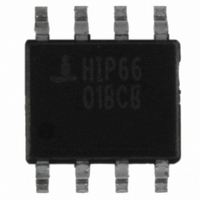
HIP6601BCB Intersil, HIP6601BCB Datasheet - Page 7

HIP6601BCB
Manufacturer Part Number
HIP6601BCB
Description
IC DRIVER MOSFET DUAL 8-SOIC
Manufacturer
Intersil
Datasheet
1.HIP6601BCBZA.pdf
(11 pages)
Specifications of HIP6601BCB
Configuration
High and Low Side, Synchronous
Input Type
PWM
Current - Peak
400mA
Number Of Configurations
1
Number Of Outputs
2
High Side Voltage - Max (bootstrap)
15V
Voltage - Supply
10.8 V ~ 13.2 V
Operating Temperature
0°C ~ 85°C
Mounting Type
Surface Mount
Package / Case
8-SOIC (3.9mm Width)
Lead Free Status / RoHS Status
Contains lead / RoHS non-compliant
Delay Time
-
Available stocks
Company
Part Number
Manufacturer
Quantity
Price
Part Number:
HIP6601BCB
Manufacturer:
INTERSIL
Quantity:
20 000
Company:
Part Number:
HIP6601BCB-T
Manufacturer:
ITS
Quantity:
4 253
Company:
Part Number:
HIP6601BCB-T
Manufacturer:
RENESAS
Quantity:
4 932
Part Number:
HIP6601BCB-T
Manufacturer:
INTRESIL
Quantity:
20 000
Part Number:
HIP6601BCBZ
Manufacturer:
INTERSIL
Quantity:
20 000
Company:
Part Number:
HIP6601BCBZ-T
Manufacturer:
INTERSIL
Quantity:
37 500
Part Number:
HIP6601BCBZ-T
Manufacturer:
INTERSIL
Quantity:
20 000
be performed to ensure safe operation at the desired
frequency for the selected MOSFETs. The power dissipated
by the driver is approximated as:
where f
and V
and Q
MOSFET selection and any external capacitance added to
the gate pins. The I
of the driver and is typically 30mW.
The power dissipation approximation is a result of power
transferred to and from the upper and lower gates. But, the
internal bootstrap device also dissipates power on-chip
during the refresh cycle. Expressing this power in terms of
the upper MOSFET total gate charge is explained below.
The bootstrap device conducts when the lower MOSFET or
its body diode conducts and pulls the PHASE node toward
GND. While the bootstrap device conducts, a current path is
formed that refreshes the bootstrap capacitor. Since the
upper gate is driving a MOSFET, the charge removed from
the bootstrap capacitor is equivalent to the total gate charge
of the MOSFET. Therefore, the refresh power required by
the bootstrap capacitor is equivalent to the power used to
charge the gate capacitance of the MOSFET.
where Q
capacitor and provided to the upper gate load.
The 1.05 factor is a correction factor derived from the
following characterization. The base circuit for characterizing
the drivers for different loading profiles and frequencies is
provided. C
capacitors. Decoupling capacitors [0.15µF] are added to the
PVCC and VCC pins. The bootstrap capacitor value is
0.01µF.
In Figure 1, C
is varied from 50kHz to 2MHz. PVCC and VCC are tied
together to a +12V supply. Curves do exceed the 800mW
cutoff, but continuous operation above this point is not
recommended.
Figure 2 shows the dissipation in the driver with 3nF loading
on both gates and each individually. Note the higher upper
gate power dissipation which is due to the bootstrap device
refresh cycle. Again PVCC and VCC are tied together and to
a +12V supply.
P
P
REFRESH
=
1.05f
L
L
sw
represent the upper and lower gate rail voltage. Q
is the upper and lower gate charge determined by
LOSS
sw
is the switching frequency of the PWM signal. V
U
=
3
-- - V
2
and C
U
1
-- - f
2
is the total charge removed from the bootstrap
U
and C
SW
Q
U
DDQ
Q
L
+
LOSS
are the upper and lower gate load
V
L
L
values are the same and frequency
V
Q
CC
L
V
PVCC
+
product is the quiescent power
7
I
DDQ
=
VCC
1
-- - f
2
SW
Q
HIP6601B, HIP6603B, HIP6604B
U
V
U
U
U
Test Circuit
The impact of loading on power dissipation is shown in
Figure 3. Frequency is held constant while the gate capacitors
are varied from 1nF to 5nF. VCC and PVCC are tied together
and to a +12V supply. Figures 4, 5 and 6 show the same
characterization for the HIP6603B with a +5V supply on PVCC
and VCC tied to a +12V supply.
Since both upper and lower gate capacitance can vary,
Figure 8 shows dissipation curves versus lower gate
capacitance with upper gate capacitance held constant at three
different values. These curves apply only to the HIP6601B due
to power supply configuration.
+12V
1000
1000
FIGURE 1. POWER DISSIPATION vs FREQUENCY
800
600
400
200
800
600
400
200
0.15µF
0.15µF
+5V OR +12V
0
0
VCC = PVCC = 12V
C
U
FIGURE 2. 3nF LOADING PROFILE
= C
C
U
PVCC
PWM
L
= C
VCC
= 3nF
500
500
L
+5V OR +12V
= 3nF
C
C
U
U
FREQUENCY (kHz)
FREQUENCY (kHz)
BOOT
= C
= C
GND
L
L
0.01µF
UGATE
PHASE
LGATE
= 4nF
= 5nF
1000
1000
C
C
C
U
L
2N7002
L
= 0nF
= 3nF
VCC = PVCC = 12V
C
C
C
U
L
U
= 3nF
= 0nF
C
= C
1500
1500
U
2N7002
L
= C
= 1nF
L
100kΩ
= 2nF
July 20, 2005
C
FN9072.7
2000
2000
U


