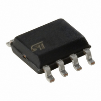
E-L6385D013TR STMicroelectronics, E-L6385D013TR Datasheet

E-L6385D013TR
Specifications of E-L6385D013TR
Related parts for E-L6385D013TR
E-L6385D013TR Summary of contents
Page 1
... CC UV DETECTION 2 HIN 1 LIN November 2003 SO8 pendent referenced N Channel Power MOS or IGBT. The Upper (Floating) Section is enabled to work with voltage Rail up to 600V. The Logic In- puts are CMOS/TTL compatible for ease of inter- facing with controlling devices. UV DETECTION LEVEL LOGIC SHIFTER ...
Page 2
... Logic Input Voltage dVout/dt Allowed Output Slew Rate Ptot Total Power Dissipation ( °C) Tj Junction Temperature Ts Storage Temperature Note: ESD immunity for pins 6, 7 and 8 is guaranteed up to 900V (Human Body Model) PIN CONNECTION THERMAL DATA Symbol R Thermal Resistance Junction to Ambient th j-amb PIN DESCRIPTION N. ...
Page 3
... Floating Supply Voltage Vout fsw Switching Frequency Vcc 2 Supply Voltage T Junction Temperature j Note 1: If the condition Vboot - Vout < 18V is guaranteed, Vout can range from -3 to 580V. ELECTRICAL CHARACTERISTICS AC Operation (Vcc = 15V 25°C) Symbol Pin Parameter ton High/Low Side Driver Turn-On Propagation Delay toff ...
Page 4
... C (nF) 0 This capacitor C gate charge : The ratio between the capacitors C is proportional to the cyclical voltage loss . It has to be: e.g 3nF. With 300mV. value the external If HVG has to be supplied for a long time, the C BOOT D99IN1053 Voltage related to the MOS total ...
Page 5
... This structure can work only if V GND (or lower) and in the meanwhile the LVG is on. The charging time (T charge the time in which both conditions are fulfilled and it has to be long enough to charge the capacitor. The bootstrap driver introduces a voltage drop due to the DMOS R DSON Ohm) ...
Page 6
... Typ -45 - Figure 9. Vcc UV Turn On Threshold vs. Temperature Typ -45 - (°C) 6/9 Figure 10. Vcc UV Turn Off Threshold vs Vcc = 15V 100 125 -45 Figure 11. Output Source Current vs. Tem- 1000 @ Vcc = 15V 800 600 400 200 0 75 100 125 Figure 12. Output Sink Current vs. Tempera- 1000 800 600 ...
Page 7
... D 10.92 E 7.95 9.75 0.313 e 2.54 e3 7.62 e4 7.62 F 6.6 I 5.08 L 3.18 3.81 0.125 Z 1.52 inch TYP. MAX. 0.131 0.065 0.022 0.012 0.430 0.384 0.100 0.300 0.300 0.260 0.200 0.150 0.060 OUTLINE AND MECHANICAL DATA Minidip L6385 7/9 ...
Page 8
... L 0.40 1.27 0.016 k 0˚ (min.), 8˚ (max.) ddd 0.10 Note: (1) Dimensions D does not include mold flash, protru- sions or gate burrs. Mold flash, potrusions or gate burrs shall not exceed 0.15mm (.006inch) in total (both side). 8/9 inch TYP. MAX. MECHANICAL DATA ...
Page 9
... STMicroelectronics. The ST logo is a registered trademark of STMicroelectronics. Australia – Belgium - Brazil - Canada - China – Czech Republic - Finland - France - Germany - Hong Kong - India - Israel - Italy - Japan - Malaysia - Malta - Morocco - Singapore - Spain - Sweden - Switzerland - United Kingdom - United States All other names are the property of their respective owners © ...


