IR2011 International Rectifier, IR2011 Datasheet
IR2011
Specifications of IR2011
Available stocks


Related parts for IR2011

IR2011 Summary of contents
Page 1
... Other high frequency applications Description The IR2011 is a high power, high speed power MOSFET driver with independent high and low side referenced output channels, ideal for Audio Class D and DC-DC converter applications. Logic inputs are compatible with standard CMOS or LSTTL output, down to 3 ...
Page 2
... IR2011(S) & (PbF) Absolute Maximum Ratings Absolute maximum ratings indicate sustained limits beyond which damage to the device may occur. All voltage param- eters are absolute voltages referenced to COM. The thermal resistance and power dissipation ratings are measured under board mounted and still air conditions. ...
Page 3
... COM and are O O Min. Typ. Max. Units Test Conditions 2.2 — — BIAS O — O — — — — — 8.2 7.4 8.2 7.4 — — IR2011(S) & (PbF) 80 — — 200V — 20 — 20 and I parameters are referenced — ...
Page 4
... IR2011(S) & (PbF) Functional Block Diagram 3V S-TRIGGER LOW VOLTAGE HIN LEVEL SHIFT 3V S-TRIGGER LOW VOLTAGE LIN LEVEL SHIFT Lead Definitions Symbol Description HIN Logic input for high side gate driver output (HO), in phase LIN Logic input for low side gate driver output (LO), in phase ...
Page 5
... DM1 Figure 1. Timing Diagram IR2011(S) & (PbF) 50% HIN / LIN t fall 90% t (H) off HO 10% DM2 90% t (L) off LO 5 ...
Page 6
... IR2011(S) & (PbF) 500 400 300 200 100 T yp. 0 -50 - Temperature ( Figure 2A. Turn-on Propagation Delay vs. Temperature 500 400 300 200 100 Typ. 0 -50 - Temperature ( Figure 3A. Turn-off Propagation Delay vs. Temperature 6 500 400 300 200 Typ. 100 0 75 100 125 Figure 2B. Turn-on Propagation Delay ...
Page 7
... Figure 4A. Turn-on Rise Time vs. Temperature 50 40 Max. 30 Typ -50 - Temperature ( Figure 5A. Turn-off Fall Time vs. Temperature www.irf.com 100 80 Max. 60 Typ 100 125 10 C) Figure 4B. Turn-on Rise Time vs. Supply Voltage 50 Max Typ 100 125 Figure 5B. Turn-off Fall Time vs. Supply Voltage IR2011(S) & (PbF Supply Voltage ( Supply Voltage ( ...
Page 8
... IR2011(S) & (PbF Max Typ. 0 -50 - Temperature ( C) Figure 6A. Turn-on Delay Matching Time vs. Temperature Max Typ. 0 -50 - Temperature ( C) Figure 7A. Turn-off Delay Matching Time vs. Temperature Max Typ 100 125 10 Figure 6B. Turn-on Delay Matching Time Max Typ 100 125 10 Figure 7B. Turn-off Delay Matching Time ...
Page 9
... Figure 8A. Logic "1" Input Voltage vs. Temperature Max -50 - Temperature ( C) Figure 9A. Logic "0" Input Voltage vs. Temperature www.irf.com Min 100 125 Figure 8B. Logic "1" Input Voltage Max 100 125 Figure 9B. Logic "0" Input Voltage IR2011(S) & (PbF Supply Voltage (V) vs. Supply Voltage Supply Voltage (V) vs. Supply Voltage ...
Page 10
... IR2011(S) & (PbF Max -50 - Temperature ( C) Figure 10A. High Level Output vs.Temperature 0.5 0.4 0.3 0.2 Max. 0.1 0.0 -50 - Temperature ( Figure 11A. Low Level Output vs. Temperature Max 100 125 Figure 10B. High Level Output vs. Supply Voltage 0.5 0.4 0.3 0.2 Max. 0.1 ...
Page 11
... Max. 0 Typ. -50 - Temperature ( www.irf.com 500 400 300 200 100 0 75 100 125 600 500 400 300 200 100 Max. 0 Typ. 75 100 125 IR2011(S) & (PbF) Max. 80 110 140 170 V Boost Voltage ( Floating Supply Voltage (V) BS 200 20 11 ...
Page 12
... IR2011(S) & (PbF) 600 500 400 300 Max. 200 Typ. 100 0 -50 - Temperature ( Figure 14A. V Supply Current CC vs. Tem perature 100 Max. Typ. 0 -50 - Temperature ( Figure 15A. Logic "1" Input Bias Current vs. Tem perature 12 600 500 400 300 200 Max. 100 Typ ...
Page 13
... V Undervoltage Threshold (+) CC BS vs. Temperature www.irf.com Max 100 125 10 C) Figure 16B. Logic "0" Input Bias Current Max. 9 Typ. 8 Min 100 125 -50 -25 C) Figure 18. V IR2011(S) & (PbF Supply Voltage (V) vs. Supply Voltage 100 o Temperature ( C) and V Undervoltage Threshold (-) CC BS vs. Temperature 20 125 13 ...
Page 14
... IR2011(S) & (PbF Typ -50 - Temperature ( Figure19A. Output Source Current vs. Temperature Typ. 0 -50 - Temperature ( Figure 20A. Output Sink Current vs. Temperature Typ 100 125 10 C) Figure 19B. Output Source Current Typ 100 125 Supply Voltage (V) vs. Supply Voltage Supply Voltage (V) Figure 20B. Output Sink Current vs ...
Page 15
... Typ Floating Supply Voltage (V) BS Figure 21. Maximum V Negative Offset S vs. V Floating Supply Voltage BS IR2011(S) & (PbF ...
Page 16
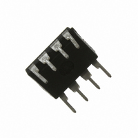
... IR2011(S) & (PbF) Case outlines 0.25 [.010 0.25 [.010 NOTES: 1. DIMENSIONING & TOLERANCING PER ASME Y14.5M-1994. 2. CONTROLLING DIMENSION: MILLIMETER 3. DIMENSIONS ARE SHOWN IN MILLIMETERS [INCHES]. 4. OUTLINE CONFORMS TO JEDEC OUTLINE MS-012AA. 16 8-Lead PDIP FOOTPRINT 8X 0.72 [.028 6.46 [.255] 3X 1.27 [.050] 8X 1.78 [.070 45° ...
Page 17
... IR2011(S) & (PbF) IRxxxxxx YWW? ?XXXX (Prod mode - 4 digit SPN code) Assembly site code Per SCOP 200-002 Leadfree Part 8-Lead PDIP IR2011 order IR2011PbF 8-Lead SOIC IR2011S order IR2011SPbF Data and specifications subject to change without notice IR logo Lot Code http://www.irf.com/ 3/4/2008 . ...