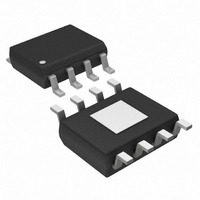
MAX15019AASA+T Maxim Integrated Products, MAX15019AASA+T Datasheet - Page 11

MAX15019AASA+T
Manufacturer Part Number
MAX15019AASA+T
Description
IC MOSF DRVR HALF BRDG HS 8-SOIC
Manufacturer
Maxim Integrated Products
Type
High Side/Low Sider
Datasheet
1.MAX15019BASA.pdf
(14 pages)
Specifications of MAX15019AASA+T
Configuration
Half Bridge
Input Type
Non-Inverting
Delay Time
36ns
Current - Peak
3A
Number Of Configurations
1
Number Of Outputs
2
High Side Voltage - Max (bootstrap)
125V
Voltage - Supply
8 V ~ 12.6 V
Operating Temperature
-40°C ~ 125°C
Mounting Type
Surface Mount
Package / Case
8-SOIC (3.9mm Width) Exposed Pad, 8-eSOIC. 8-HSOIC
Rise Time
50 ns
Fall Time
40 ns
Supply Voltage (min)
8 V
Supply Current
2.75 mA
Maximum Power Dissipation
1904 mW
Maximum Operating Temperature
+ 125 C
Mounting Style
SMD/SMT
Bridge Type
Half Bridge
Maximum Turn-off Delay Time
36 ns
Maximum Turn-on Delay Time
36 ns
Minimum Operating Temperature
- 40 C
Number Of Drivers
2
Lead Free Status / RoHS Status
Lead free / RoHS Compliant
The MAX15018_/MAX15019_ drivers source and sink
large currents to create very fast rise and fall edges at
the gates of the switching MOSFETs. The high di/dt can
cause unacceptable ringing if the trace lengths and
impedances are not well controlled. Use the following
PCB layout guidelines when designing with the
MAX15018_/MAX15019_:
• It is important that the V
• There are two AC current loops formed between the
Figure 2. Half-Bridge Converter Application with Secondary-Side Synchronous Rectification
ground) or BST voltage (with respect to HS) does not
exceed 15V. Voltage spikes higher than 15V from
V
device. Place one or more low-ESL 0.1µF decoupling
ceramic capacitors from V
to HS as close as possible to the part. The ceramic
decoupling capacitors should be at least 20 times
the gate capacitance being driven.
IC and the gate of the MOSFET being driven. The
PWM1
PWM2
DD
V
DD
to GND or from BST to HS can damage the
= 8V TO 12.6V
IN_H
IN_L
______________________________________________________________________________________
V
DD
MAX15018A
GND
DD
DD
BST
Layout Information
voltage (with respect to
to GND and from BST
DH
HS
DL
Half-Bridge MOSFET Drivers
N
N
V
• Solder the exposed pad of the 8-pin SO-EP package
IN
= 0 TO 125V
MOSFET looks like a large capacitance from gate to
source when the gate is being pulled low. The active
current loop is from the MOSFET driver output (DL or
DH) to the MOSFET gate, to the MOSFET source, and
to the return terminal of the MOSFET driver (either
GND or HS). When the gate of the MOSFET is being
pulled high, the active current loop is from the MOS-
FET driver output, (DL or DH), to the MOSFET gate, to
the MOSFET source, to the return terminal of the dri-
vers decoupling capacitor, to the positive terminal of
the decoupling capacitor, and to the supply connec-
tion of the MOSFET driver. The decoupling capacitor
will be either C
V
Care must be taken to minimize the physical distance
and the impedance of these AC current paths.
to a large copper plane to achieve the rated power
dissipation.
125V/3A, High-Speed,
DD
decoupling capacitor for the low-side MOSFET.
Typical Application Circuits
BST
N
N
for the high-side MOSFET or the
V
OUT
11


