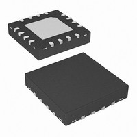
ISL6210CRZ Intersil, ISL6210CRZ Datasheet - Page 5

ISL6210CRZ
Manufacturer Part Number
ISL6210CRZ
Description
IC MOSFET DRIVER DUAL SYNC 16QFN
Manufacturer
Intersil
Datasheet
1.ISL6210CRZ.pdf
(10 pages)
Specifications of ISL6210CRZ
Configuration
High and Low Side, Synchronous
Input Type
PWM
Delay Time
26ns
Current - Peak
2A
Number Of Configurations
2
Number Of Outputs
4
High Side Voltage - Max (bootstrap)
36V
Voltage - Supply
4.5 V ~ 5.5 V
Operating Temperature
-10°C ~ 100°C
Mounting Type
Surface Mount
Package / Case
16-VQFN Exposed Pad, 16-HVQFN, 16-SQFN, 16-DHVQFN
Lead Free Status / RoHS Status
Lead free / RoHS Compliant
Available stocks
Company
Part Number
Manufacturer
Quantity
Price
Company:
Part Number:
ISL6210CRZ
Manufacturer:
NDK
Quantity:
3 924
Functional Pin Description
Electrical Specifications
NOTE:
OUTPUT
Upper Drive Source Resistance
Upper Drive Source Current (Note 4)
Upper Drive Sink Resistance
Upper Drive Sink Current (Note 4)
Lower Drive Source Resistance
Lower Drive Source Current (Note 4)
Lower Drive Sink Resistance
Lower Drive Sink Current (Note 4)
NUMBER
3. Parameters with MIN and/or MAX limits are 100% tested at +25°C, unless otherwise specified. Temperature limits established by characterization
4. Limits established by characterization and are not production tested.
N/A
and are not production tested.
10
11
12
13
14
15
16
1
2
3
4
5
6
7
8
9
PHASE2 Connect this pin to the SOURCE of the upper MOSFET and the DRAIN of the lower MOSFET in Channel 2. This pin
UGATE2 Upper gate drive output of Channel 2. Connect to gate of high-side power N-Channel MOSFET.
UGATE1 Upper gate drive output of Channel 1. Connect to gate of high-side power N-Channel MOSFET.
PHASE1 Connect this pin to the SOURCE of the upper MOSFET and the DRAIN of the lower MOSFET in Channel 1. This pin
LGATE1 Lower gate drive output of Channel 1. Connect to gate of the low-side power N-Channel MOSFET.
LGATE2 Lower gate drive output of Channel 2. Connect to gate of the low-side power N-Channel MOSFET.
BOOT2
BOOT1
NAME
PWM1
PWM2
PVCC
FCCM
PGND
GND
VCC
PAD
PARAMETER
EN
Bias and reference ground. All signals are referenced to this node.
This pin supplies power to both the lower and higher gate drives in ISL6210. Connect to a +5V supply. Place a high quality
low ESR ceramic capacitor from this pin to GND.
Logic control input that will force continuous conduction mode (HIGH state) or allow discontinuous conduction mode
(LOW state). Placing a series resistor in this input will allow the switching dead-time to be programmed.
It is the power ground return of both low gate drivers.
Logic control input that will enable (HIGH state) or disable (LOW state) the IC. Shutdown current is <1µA.
provides a return path for the upper gate drive.
Floating bootstrap supply pin for the upper gate drive of Channel 2. Connect the bootstrap capacitor between this pin and
the PHASE2 pin. The bootstrap capacitor provides the charge to turn on the upper MOSFET. See “Internal Bootstrap Diode”
on page 7 for guidance in choosing the capacitor value.
Floating bootstrap supply pin for the upper gate drive of Channel 1. Connect the bootstrap capacitor between this pin and
the PHASE1 pin. The bootstrap capacitor provides the charge to turn on the upper MOSFET. See“Internal Bootstrap Diode”
on page 7 for guidance in choosing the capacitor value.
provides a return path for the upper gate drive.
Connect a +5V bias supply to this pin. It supplies the internal analog circuits. Place a high quality, low ESR ceramic capacitor
from this pin to GND. This should be a separate capacitor than the one used for PVCC (Pin 3).
The PWM signal is the control input for the Channel 1 driver. The PWM signal can enter three distinct states during operation. See
“Three-State PWM Input” on page 6 for further details. Connect this pin to the PWM output of the controller.
The PWM signal is the control input for the Channel 2 driver. The PWM signal can enter three distinct states during operation. See
“Three-State PWM Input” on page 6 for further details. Connect this pin to the PWM output of the controller.
Connect this pad to the power ground plane (GND) via thermally enhanced connection.
5
These specifications apply for T
MIN and/or MAX limits are 100% tested at +25°C, unless otherwise specified. Temperature limits established by
characterization and are not production tested.
R
R
SYMBOL
R
R
I
I
I
I
UG_SCR
UG_SNK
LG_SCR
LG_SNK
UG_SRC
UG_SNK
LG_SRC
LG_SNK
250mA Source Current
V
250mA Sink Current
V
250mA Source Current
V
250mA Sink Current
V
UGATE-PHASE
UGATE-PHASE
LGATE
LGATE
ISL6210
A
= -10°C to +100°C, Unless Otherwise Noted. (Continued)Parameters with
= 2.5V
= 2.5V
TEST CONDITIONS
= 2.5V
= 2.5V
FUNCTION
MIN
-
-
-
-
-
-
-
TYP
2.00
2.00
2.00
4.00
1.0
1.0
1.0
0.4
MAX
2.5
2.5
2.5
1.0
-
-
-
-
December 9, 2008
UNITS
FN6392.1
Ω
Ω
Ω
Ω
A
A
A
A


